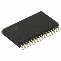
CY62128EV30LL-45SXIT Cypress Semiconductor Corp, CY62128EV30LL-45SXIT Datasheet - Page 4

CY62128EV30LL-45SXIT
Manufacturer Part Number
CY62128EV30LL-45SXIT
Description
CY62128EV30LL-45SXIT
Manufacturer
Cypress Semiconductor Corp
Datasheet
1.CY62128EV30LL-45ZXI.pdf
(15 pages)
Specifications of CY62128EV30LL-45SXIT
Format - Memory
RAM
Memory Type
SRAM
Memory Size
1M (128K x 8)
Speed
45ns
Interface
Parallel
Voltage - Supply
2.2 V ~ 3.6 V
Operating Temperature
-40°C ~ 85°C
Package / Case
32-SOIC (11.30mm Width)
Lead Free Status / RoHS Status
Lead free / RoHS Compliant
Available stocks
Company
Part Number
Manufacturer
Quantity
Price
Company:
Part Number:
CY62128EV30LL-45SXIT
Manufacturer:
CYPRESS/PBF
Quantity:
587
Maximum Ratings
Exceeding maximum ratings may shorten the useful life of the
device. User guidelines are not tested.
Storage temperature................................. –65 °C to +150 °C
Ambient temperature with
power applied ........................................... –55 °C to +125 °C
Supply voltage to ground
potential ........................................–0.3 V to V
DC voltage applied to outputs
in high Z State
Electrical Characteristics
(Over the Operating Range)
Notes
Document #: 38-05579 Rev. *I
V
V
V
V
I
I
I
I
I
Parameter
4. V
5. V
6. Full device AC operation assumes a 100
7. Typical values are included for reference only and are not guaranteed or tested. Typical values are measured at V
8. Chip enables (CE
IX
OZ
CC
SB1
SB2
OH
OL
IH
IL
[8]
IL(min)
IH(max)
= –2.0 V for pulse durations less than 20 ns.
= V
CC
Output HIGH voltage
Output LOW voltage
Input HIGH voltage
Input LOW voltage
Input leakage current
Output leakage current
V
Automatic CE
power-down
current — CMOS inputs
Automatic CE
power-down
current — CMOS inputs
[4, 5]
CC
+ 0.75 V for pulse durations less than 20 ns.
1
..........................–0.3 V to V
operating supply current
and CE
Description
2
) must be at CMOS level to meet the I
µ
s ramp time from 0 to V
CC(max)
CC(max)
I
I
I
I
V
V
V
V
GND < V
GND < V
f = f
f = 1 MHz
CE
V
f = f
f = 0 (OE and WE), V
CE
V
f = 0, V
OH
OH
OL
OL
CC
CC
CC
CC
IN
IN
1
1
= 0.1 mA
= 2.1 mA, V
max
> V
max
= –0.1 mA
= –1.0 mA, V
> V
= 2.7 V to 3.6 V
= 2.7 V to 3.6 V
= 2.2 V to 2.7 V
= 2.2 V to 2.7 V
> V
> V
+ 0.3 V
+ 0.3 V
CC
CC
CC
(address and data Only),
= 1/t
SB2
CC
CC
CC
I
O
< V
< V
– 0.2 V, V
= 3.60 V
(min) and 200
– 0.2 V or V
0.2 V, CE
/ I
– 0.2 V, CE
RC
CCDR
Test Conditions
CC
CC
CC
, output disabled
CC
spec. Other inputs can be left floating.
> 2.70 V
> 2.70 V
IN
DC input voltage
Output current into outputs (LOW) .............................. 20 mA
Static discharge voltage.......................................... > 2001 V
(MIL-STD-883, method 3015)
Latch-up current ..................................................... > 200 mA
Operating Range
V
0 mA CMOS levels
CC
CY62128EV30LL
µ
< 0.2 V
2
IN
CC
2
s wait time after V
< 0.2 V
= 3.60 V
< 0.2 V
< 0.2 V,
= V
Device
CCmax
I
OUT
CC
[4, 5]
stabilization.
=
......................–0.3 V to V
Industrial
Range
CC
–0.3
–0.3
Min
2.0
2.4
1.8
2.2
–1
–1
= V
CY62128EV30 MoBL
–
–
–
–
–
–
CC(typ)
45 ns (Industrial)
, T
–40 °C to +85 °C 2.2 V to
Typ
A
1.3
Temperature
11
= 25 °C.
–
–
–
–
–
–
–
–
–
–
1
1
Ambient
[7]
V
V
CC(max)
CC
CC
Max
0.4
0.4
0.6
0.8
2.0
+1
+1
16
+ 0.3 V
+ 0.3 V
–
–
4
4
Page 4 of 15
+ 0.3 V
V
3.6 V
CC
Unit
mA
mA
µA
µA
µA
µA
V
V
V
V
V
V
V
V
[6]
®
[+] Feedback


