CY62157EV30LL-45BVI Cypress Semiconductor Corp, CY62157EV30LL-45BVI Datasheet - Page 3
CY62157EV30LL-45BVI
Manufacturer Part Number
CY62157EV30LL-45BVI
Description
CY62157EV30LL-45BVI
Manufacturer
Cypress Semiconductor Corp
Datasheet
1.CY62157EV30LL-45ZSXI.pdf
(17 pages)
Specifications of CY62157EV30LL-45BVI
Format - Memory
RAM
Memory Type
SRAM
Memory Size
8M (512K x 16)
Speed
45ns
Interface
Parallel
Voltage - Supply
2.2 V ~ 3.6 V
Operating Temperature
-40°C ~ 85°C
Package / Case
48-VFBGA
Density
8Mb
Access Time (max)
45ns
Sync/async
Asynchronous
Architecture
Not Required
Clock Freq (max)
Not RequiredMHz
Operating Supply Voltage (typ)
2.5/3.3V
Address Bus
19b
Package Type
VFBGA
Operating Temp Range
-40C to 85C
Number Of Ports
1
Supply Current
25mA
Operating Supply Voltage (min)
2.2V
Operating Supply Voltage (max)
3.6V
Operating Temperature Classification
Industrial
Mounting
Surface Mount
Pin Count
48
Word Size
16b
Number Of Words
512K
Lead Free Status / RoHS Status
Contains lead / RoHS compliant by exemption
Lead Free Status / RoHS Status
Contains lead / RoHS compliant by exemption
Available stocks
Company
Part Number
Manufacturer
Quantity
Price
Company:

Part Number:
CY62157EV30LL-45BVI
Manufacturer:
Cypress Semiconductor Corp
Quantity:
10 000
Company:
Part Number:
CY62157EV30LL-45BVIT
Manufacturer:
Cypress Semiconductor Corp
Quantity:
10 000


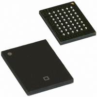
Pin Configuration
Figure 1. 48-Ball VFBGA (Top View)
Product Portfolio
Document #: 38-05445 Rev. *H
Notes
CY62157EV30LL
1. Typical values are included for reference only and are not guaranteed or tested. Typical values are measured at V
2. NC pins are not connected on the die.
3. The 44-TSOP II package has only one chip enable (CE) pin.
4. The BYTE pin in the 48-TSOP I package must be tied HIGH to use the device as a 512K × 16 SRAM. The 48-TSOP I package can also be used as a 1M × 8
SRAM by tying the BYTE signal LOW. In the 1M x 8 configuration, Pin 45 is A19, while BHE, BLE and I/O8 to I/O14 pins are not used (NC).
Product
BLE
I/O
I/O
I/O
V
V
I/O
A
CC
1
SS
18
14
15
8
9
I/O
BHE
I/O
I/O
I/O
OE
NC
A
2
11
8
10
12
13
Industrial/
Range
Auto-A
Auto-E
A
A
NC
A
A
A
A
A
3
17
14
12
0
3
5
9
A
A
A
A
A
A
A15
A14
A13
A12
A11
A10
A9
A8
NC
NC
WE
CE2
NC
BHE
BLE
A18
A17
A7
A6
A5
A4
A3
A2
A1
A
A
4
16
15
13
10
4
7
1
6
Figure 3. 48-Pin TSOP I (512K x 16/1M x 8) (Top View)
1
2
3
4
5
6
7
8
9
10
11
12
13
14
15
16
17
18
19
20
21
22
23
24
I/O
CE
I/O
I/O
I/O
WE
A
A
[2]
5
11
Min
2
2.2
2.2
3
1
1
4
5
V
CE
I/O
V
V
I/O
I/O
I/O
NC
6
CC
CC
SS
2
0
2
6
7
Typ
Range (V)
3.0
3.0
A
D
E
G
H
B
C
F
[1]
Max
3.6
3.6
Speed
(ns)
Figure 2. 44-Pin TSOP II (Top View)
45
55
Typ
1.8
1.8
f = 1 MHz
[1]
Operating I
Max
V
V
WE
A
A
A
A
A
I/O
I/O
I/O
I/O
I/O
I/O
I/O
I/O
CE
A
A
A
A
A
CC
3
4
SS
18
15
14
17
16
3
0
4
2
1
1
2
4
5
7
0
3
6
48
47
46
45
44
43
42
41
40
39
38
37
36
35
34
33
32
31
30
29
28
27
26
25
Power Dissipation
11
12
10
13
14
15
16
17
18
19
20
21
22
Typ
CC
1
2
3
4
5
6
7
8
9
[2, 4]
CC
A16
BYTE
Vss
I/O15/A19
I/O7
I/O14
I/O6
I/O13
I/O5
I/O12
I/O4
Vcc
I/O11
I/O3
I/O10
I/O2
I/O9
I/O1
I/O8
I/O0
OE
Vss
CE1
A0
18
18
CY62157EV30 MoBL
= V
, (mA)
f = f
[1]
CC(typ)
max
Max
, T
25
35
44
43
42
41
40
39
38
37
36
35
34
33
32
31
30
29
28
27
26
25
24
23
A
= 25°C.
[3]
A
A
A
OE
BHE
BLE
I/O
I/O
I/O
I/O
V
V
I/O
I/O
I/O
I/O
A
A
A
A
A
A
Typ
Standby, I
5
6
7
SS
CC
8
9
10
11
12
13
15
14
13
12
11
10
9
8
2
2
[1]
(A)
Page 3 of 17
Max
30
SB2
8
®
[+] Feedback
Related parts for CY62157EV30LL-45BVI
Image
Part Number
Description
Manufacturer
Datasheet
Request
R

Part Number:
Description:
8-mbit 512k X 16 Static Ram
Manufacturer:
Cypress Semiconductor Corporation.
Datasheet:

Part Number:
Description:
Manufacturer:
Cypress Semiconductor Corp
Datasheet:
Part Number:
Description:
Manufacturer:
Cypress Semiconductor Corp
Datasheet:
Part Number:
Description:
Manufacturer:
Cypress Semiconductor Corp
Datasheet:
Part Number:
Description:
Manufacturer:
Cypress Semiconductor Corp
Datasheet:
Part Number:
Description:
Manufacturer:
Cypress Semiconductor Corp
Datasheet: