CY7B994V-5BBC Cypress Semiconductor Corp, CY7B994V-5BBC Datasheet - Page 5

CY7B994V-5BBC
Manufacturer Part Number
CY7B994V-5BBC
Description
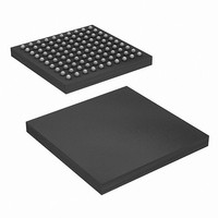
IC,Sixteen Distributed-Output Clock Driver,BGA,100PIN,PLASTIC
Manufacturer
Cypress Semiconductor Corp
Series
RoboClock™r
Type
Clock Buffer, Fanout Distributionr
Datasheet
1.CY7B993V-2AXC.pdf
(18 pages)
Specifications of CY7B994V-5BBC
Pll
Yes
Input
LVPECL, LVTTL
Output
LVTTL
Number Of Circuits
1
Ratio - Input:output
4:18
Differential - Input:output
No/No
Frequency - Max
200MHz
Divider/multiplier
Yes/Yes
Voltage - Supply
2.97 V ~ 3.63 V
Operating Temperature
0°C ~ 70°C
Mounting Type
Surface Mount
Package / Case
100-LBGA
Frequency-max
200MHz
Lead Free Status / RoHS Status
Contains lead / RoHS non-compliant
Available stocks
Company
Part Number
Manufacturer
Quantity
Price
Company:
Part Number:
CY7B994V-5BBC
Manufacturer:
CY
Quantity:
2 286
Company:
Part Number:
CY7B994V-5BBC
Manufacturer:
CYPRESS
Quantity:
219
Company:
Part Number:
CY7B994V-5BBC
Manufacturer:
Cypress Semiconductor Corp
Quantity:
10 000
Company:
Part Number:
CY7B994V-5BBCT
Manufacturer:
CYPRESS
Quantity:
213
Company:
Part Number:
CY7B994V-5BBCT
Manufacturer:
Cypress Semiconductor Corp
Quantity:
10 000
Pinouts
Table 1. Pin Definition
Document #: 38-07127 Rev. *I
FBSEL
FBKA+, FBKA–
FBKB+, FBKB–
REFA+, REFA–
REFB+, REFB–
REFSEL
FS
FBF0
Note
1. For all three-state inputs, HIGH indicates a connection to V
circuitry holds an unconnected input to V
Pin Name
(continued)
A
B
C
D
E
F
G
H
J
K
(3_level)
(3_level)
VCCN
LOCK
1QB1
4QB1
4QB0
4QA1
4QA0
4DS0
Input
Input
Input
Input
Input
Input
GND
2F1
1
I/O
[1]
(3_level)
(3_level) VCCQ
(3_level)
(3_level)
(3_level)
VCCN
VCCN
VCCN
1QB0
2DS1
1DS1
3DS0
Pin Type
LVTTL
LVTTL/
LVDIFF
LVTTL/
LVDIFF
LVTTL
3-level
Input
3-level
Input
GND
4F0
1F1
2
CC
(3_level)
(3_level)
(3_level)
(3_level) VCCQ
(3_level)
VCCN
1QA1
4DS1
3DS1
1DS0
2DS0
/2.
GND
DIS2
3F1
Feedback Input Select. When LOW, FBKA inputs are selected. When HIGH, the FBKB
inputs are selected. This input has an internal pull-down.
Feedback Inputs. One pair of inputs selected by the FBSEL is used to feedback the clock
output xQn to the phase detector. The PLL operates such that the rising edges of the
reference and feedback signals are aligned in both phase and frequency. These inputs
can operate as differential PECL or single-ended TTL inputs. When operating as a
single-ended LVTTL input, the complementary input must be left open.
Reference Inputs. These inputs can operate as differential PECL or single-ended TTL
reference inputs to the PLL. When operating as a single-ended LVTTL input, the comple-
mentary input must be left open.
Reference Select Input. The REFSEL input controls how the reference input is
configured. When LOW, it uses the REFA pair as the reference input. When HIGH, it uses
the REFB pair as the reference input. This input has an internal pull-down.
Frequency Select. This input must be set according to the nominal frequency (f
Table
Feedback Output Phase Function Select. This input determines the phase function of
the Feedback bank’s QFA[0:1] outputs (see
3
Figure 2. Pin Diagram – 100-Pin BGA
2).
VCCN
VCCN
1QA0
GND
GND
GND
GND
GND
DIS1
4
CC
, LOW indicates a connection to GND, and MID indicates an open connection. Internal termination
(3_level)
(3_level)
FBDS1
VCCN
VCCN
QFA0
3QA0
GND
GND
GND
GND
3F0
5
(3_level)
(3_level)
FBDS0
VCCN
VCCN
QFA1
3QA1
GND
GND
GND
GND
4F1
6
(3_level)
FBKB+
VCCQ
VCCQ
VCCQ
GND
GND
GND
GND
GND
2F0
Pin Description
7
OUTPUT
(3_level)
(3_level)
(3_level)
(3_level)
FBKB–
MODE
VCCQ
VCCQ REFSEL REFB–
VCCQ
3QB0
FBF0
GND
INV3
FS
Table
8
4).
(3_level)
FBKA–
FBSEL
FBDIS
VCCN
VCCN
3QB1
GND
DIS3
1F0
9
CY7B993V, CY7B994V
FBKA+
REFA+
REFB+
REFA–
2QA1
2QB0
2QA0
2QB1
DIS4
10
RoboClock
NOM
Page 5 of 18
) (see
[+] Feedback


