CY7C1019CV33-10ZXA Cypress Semiconductor Corp, CY7C1019CV33-10ZXA Datasheet
CY7C1019CV33-10ZXA
Specifications of CY7C1019CV33-10ZXA
Available stocks


Related parts for CY7C1019CV33-10ZXA


CY7C1019CV33-10ZXA Summary of contents
Page 1
... Document #: 38-05130 Rev Mbit (128K x 8) Static RAM Functional Description The CY7C1019CV33 is a high performance CMOS static RAM organized as 131,072 words by 8 bits. Easy memory expansion is provided by an active LOW Chip Enable (CE), an active LOW Output Enable (OE), and tristate drivers. This device has an automatic power down feature that significantly reduces power consumption when deselected ...
Page 2
... Maximum Access Time Maximum Operating Current Maximum Standby Current Pin Configuration Figure 1. 32-Pin SOJ/TSOP II (Top View Note 1. NC pins are not connected on the die. Document #: 38-05130 Rev. *J -10 (Industrial/ -12 (Industrial) Auto- [ I I CY7C1019CV33 -15 (Industrial) Unit Page [+] Feedback ...
Page 3
... MAX , 5 CC – 0.3V, CC – 0.3V, CC < 0.3V Test Conditions MHz 5.0V CC CY7C1019CV33 Ambient V CC Temperature 3.3V ± 10 +70 C 3.3V ± 10% –40°C to +85°C 3.3V ± 10% –40°C to +85°C –15 (Industrial) Unit Min Max Min Max. 2.4 2.4 0.4 ...
Page 4
... Auto-A) Min Max Min Figure 2. 2. Transition is measured ±500 mV from steady-state voltage. Figure is less than less than t , and t HZCE LZCE HZOE LZOE and t HZWE CY7C1019CV33 [3] High-Z characteristics: R 317Ω 3.3V 10% OUTPUT 5 pF (c) -15 (Industrial) Unit Max Min Max ...
Page 5
... If CE goes HIGH simultaneously with WE going HIGH, the output remains in a high impedance state. Document #: 38-05130 Rev. *J [10, 11] Figure 3. Read Cycle No OHA DOE DATA VALID 50 SCE t SCE PWE t SD DATA VALID CY7C1019CV33 DATA VALID [11, 12] t HZOE t HZCE HIGH IMPEDANCE t PD ICC 50% ISB [13, 14 Page [+] Feedback ...
Page 6
... During this period the I/Os are in the output state and input signals should not be applied. Document #: 38-05130 Rev SCE PWE t SD DATA VALID SCE PWE t SD DATA VALID Mode 7 Power Down Read Write Selected, Outputs Disabled CY7C1019CV33 [13, 14 [14 LZWE Power Standby ( Active ( Active ( Active ( Page [+] Feedback ...
Page 7
... Ordering Information Speed Ordering Code (ns) 10 CY7C1019CV33-10ZXA CY7C1019CV33-10ZXAT Ordering Code Definitions CY7C 1019 C V33 - Document #: 38-05130 Rev. *J Package Package Type Diagram 51-85095 32-pin TSOP II (Pb-free) 51-85095 32-pin TSOP II (Pb-free Blank T = Tape and Reel; Blank = Tube Temperature Range Automotive-A Package Type 32-pin TSOP II (Pb-free) Speed Grade ( ns) V33 = 3 ...
Page 8
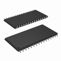
... Package Diagrams Document #: 38-05130 Rev. *J Figure 8. 32-Pin TSOP II CY7C1019CV33 51-85095 *A Page [+] Feedback ...
Page 9
... Document History Page Document Title: CY7C1019CV33 1 Mbit (128K x 8) Static RAM Document Number: 38-05130 Submission REV. ECN NO. Date ** 109245 12/16/01 *A 113431 04/10/02 *B 115047 08/01/02 *C 119796 10/11/02 *D 123030 12/17/02 *E 419983 See ECN *F 493543 See ECN *G 2761448 09/09/2009 *H 2897691 03/23/2010 *I 3057593 10/13/2010 *J 3072834 11/11/2010 Document #: 38-05130 Rev ...
Page 10
... Cypress against all charges. Use may be limited by and subject to the applicable Cypress software license agreement. Document #: 38-05130 Rev. *J All products and company names mentioned in this document may be the trademarks of their respective holders. psoc.cypress.com clocks.cypress.com image.cypress.com Revised November 11, 2010 CY7C1019CV33 Page [+] Feedback ...