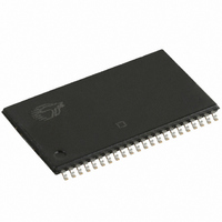
CY7C1021CV26-15ZSXET Cypress Semiconductor Corp, CY7C1021CV26-15ZSXET Datasheet - Page 4

CY7C1021CV26-15ZSXET
Manufacturer Part Number
CY7C1021CV26-15ZSXET
Description
CY7C1021CV26-15ZSXET
Manufacturer
Cypress Semiconductor Corp
Datasheet
1.CY7C1021CV26-15ZSXE.pdf
(15 pages)
Specifications of CY7C1021CV26-15ZSXET
Format - Memory
RAM
Memory Type
SRAM - Asynchronous
Memory Size
1M (64K x 16)
Speed
15ns
Interface
Parallel
Voltage - Supply
2.5 V ~ 2.7 V
Operating Temperature
-40°C ~ 125°C
Package / Case
44-TSOP II
Lead Free Status / RoHS Status
Lead free / RoHS Compliant
Maximum Ratings
Exceeding maximum ratings may shorten the useful life of the
device. User guidelines are not tested.
Storage temperature ................................ –65 C to +150 C
Ambient temperature with
power applied ........................................... –55 C to +125 C
Supply voltage on V
DC voltage applied to outputs
in high Z state
Electrical Characteristics
Over the Operating Range
Capacitance
Thermal Resistance
Document Number: 38-05589 Rev. *E
V
V
V
V
I
I
I
I
I
C
C
Notes
IX
OZ
CC
SB1
SB2
Parameter
Parameter
Parameter
3. V
4. Tested initially and after any design or process changes that may affect these parameters.
OH
OL
IH
IL
IN
OUT
IL
JC
JA
(min.) = –2.0V and V
[3]
Output HIGH voltage
Output LOW voltage
Input HIGH voltage
Input LOW voltage
Input leakage current
Output leakage current
V
Automatic CE Power-Down
Current —TTL inputs
Automatic CE Power-Down
Current —CMOS inputs
Thermal Resistance (Junction to Ambient) Still Air, soldered on a 3 × 4.5 inch,
Thermal Resistance (Junction to Case)
Input capacitance
Output capacitance
CC
................................... –0.5 V to V
[4]
operating supply current
CC
IH
(max) = V
to relative GND
Description
Description
[4]
Description
CC
[3]
+ 0.5 V for pulse durations of less than 20 ns.
[3]
.....–0.5 V to +4.6 V
V
V
GND < V
GND < V
V
Max V
Max V
or V
T
CC
CC
CC
A
CC
= 25 C, f = 1 MHz, V
IN
= Min, I
= Min, I
= Max, I
+ 0.5 V
CC
CC
< 0.3 V, f = 0
, CE > V
I
I
, CE > V
four-layer printed circuit board
< V
< V
OH
OL
OUT
CC
CC
= 1.0 mA
= –1.0 mA
, output disabled
Test Conditions
Test Conditions
= 0 mA, f = f
IH
CC
, V
DC input voltage
Current into outputs (LOW) ......................................... 20 mA
Static discharge voltage........................................... > 2001 V
(per MIL-STD-883, method 3015)
Latch-up current ..................................................... > 200 mA
Operating Range
Automotive
– 0.3 V, V
Test Conditions
IN
CC
> V
= 2.6 V
IH
Range
MAX
or V
IN
> V
= 1/t
IN
[3]
CC
< V
............................... –0.5 V to V
RC
– 0.3 V,
IL
, f = f
–40 C to +125 C
MAX
Temperature
Ambient
–0.3
Min
2.3
2.0
–3
–3
–
–
–
–
CY7C1021CV26
TSOP-II
76.92
15.86
Max
–15
8
8
V
CC
Max
0.4
0.8
+3
+3
80
15
10
–
+ 0.3
2.5 V–2.7 V
CC
Page 4 of 15
V
+ 0.5 V
CC
C/W
C/W
Unit
Unit
Unit
mA
mA
mA
A
A
pF
pF
V
V
V
V
[+] Feedback


