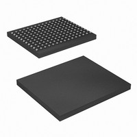
CY7C1315BV18-200BZI Cypress Semiconductor Corp, CY7C1315BV18-200BZI Datasheet - Page 11

CY7C1315BV18-200BZI
Manufacturer Part Number
CY7C1315BV18-200BZI
Description
SRAM (Static RAM)
Manufacturer
Cypress Semiconductor Corp
Datasheet
1.CY7C1313BV18-167BZC.pdf
(28 pages)
Specifications of CY7C1315BV18-200BZI
Format - Memory
RAM
Memory Type
SRAM - Synchronous, QDR II
Memory Size
18M (512K x 36)
Speed
200MHz
Interface
Parallel
Voltage - Supply
1.7 V ~ 1.9 V
Operating Temperature
-40°C ~ 85°C
Package / Case
165-LFBGA
Lead Free Status / RoHS Status
Contains lead / RoHS non-compliant
Available stocks
Company
Part Number
Manufacturer
Quantity
Price
Company:
Part Number:
CY7C1315BV18-200BZI
Manufacturer:
Cypress Semiconductor Corp
Quantity:
10 000
Document Number: 38-05620 Rev. *C
Write Cycle Descriptions
Write Cycle Descriptions
BWS
H
H
H
H
H
H
H
H
L
L
L
L
BWS
H
H
0
L
L
BWS
0
H
H
H
H
H
H
H
H
L
L
L
L
1
L–H
L–H
K
BWS
–
–
H
H
H
H
H
H
H
H
L
L
L
L
2
L–H
L–H
BWS
K
–
–
H
H
H
H
H
H
H
H
L
L
L
L
3
During the Data portion of a Write sequence, the single byte (D
During the Data portion of a Write sequence, the single byte (D
No data is written into the device during this portion of a write operation.
No data is written into the device during this portion of a write operation.
(CY7C1315BV18)
(CY7C1911BV18)
L–H
L–H
L–H
L–H
L–H
L–H
K
–
–
–
–
–
–
L–H During the Data portion of a Write sequence, all four bytes (D
L–H During the Data portion of a Write sequence, only the lower byte (D
L–H During the Data portion of a Write sequence, only the byte (D
L–H During the Data portion of a Write sequence, only the byte (D
L–H During the Data portion of a Write sequence, only the byte (D
L–H No data is written into the device during this portion of a write operation.
K
–
–
–
–
–
During the Data portion of a Write sequence, all four bytes (D
into the device.
into the device.
During the Data portion of a Write sequence, only the lower byte (D
into the device. D
into the device. D
During the Data portion of a Write sequence, only the byte (D
the device. D
the device. D
During the Data portion of a Write sequence, only the byte (D
into the device. D
into the device. D
During the Data portion of a Write sequence, only the byte (D
into the device. D
into the device. D
No data is written into the device during this portion of a write operation.
[2, 10]
[2, 10]
[8:0]
[8:0]
[35:9]
[35:9]
and D
and D
[17:0]
[17:0]
[26:0]
[26:0]
will remain unaltered.
will remain unaltered.
and D
and D
will remain unaltered.
will remain unaltered.
[35:18]
[35:18]
[35:27]
[35:27]
will remain unaltered.
will remain unaltered.
Comments
will remain unaltered.
will remain unaltered.
[8:0]
[8:0]
) is written into the device.
) is written into the device.
CY7C1313BV18
CY7C1315BV18
CY7C1311BV18
CY7C1911BV18
[17:9]
[17:9]
[35:0]
[35:0]
[26:18]
[26:18]
[35:27]
[35:27]
) is written into
) is written into
Page 11 of 28
[8:0]
[8:0]
) are written
) are written
) is written
) is written
) is written
) is written
) is written
) is written
[+] Feedback


