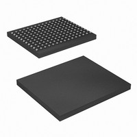
CY7C1315BV18-200BZXC Cypress Semiconductor Corp, CY7C1315BV18-200BZXC Datasheet - Page 10

CY7C1315BV18-200BZXC
Manufacturer Part Number
CY7C1315BV18-200BZXC
Description
SRAM (Static RAM)
Manufacturer
Cypress Semiconductor Corp
Datasheet
1.CY7C1315BV18-200BZXC.pdf
(32 pages)
Specifications of CY7C1315BV18-200BZXC
Format - Memory
RAM
Memory Type
SRAM - Synchronous, QDR II
Memory Size
18M (512K x 36)
Speed
200MHz
Interface
Parallel
Voltage - Supply
1.7 V ~ 1.9 V
Operating Temperature
0°C ~ 70°C
Package / Case
165-LFBGA
Lead Free Status / RoHS Status
Lead free / RoHS Compliant
Available stocks
Company
Part Number
Manufacturer
Quantity
Price
Company:
Part Number:
CY7C1315BV18-200BZXC
Manufacturer:
Cypress Semiconductor Corp
Quantity:
10 000
Concurrent Transactions
The read and write ports on the CY7C1311BV18 operate
completely independently of one another. As each port latches
the address inputs on different clock edges, the user can read or
write to any location, regardless of the transaction on the other
port. If the ports access the same location when a read follows a
write in successive clock cycles, the SRAM delivers the most
recent information associated with the specified address location.
This includes forwarding data from a write cycle that was initiated
on the previous K clock rise.
Read accesses and write access must be scheduled such that
one transaction is initiated on any clock cycle. If both ports are
selected on the same K clock rise, the arbitration depends on the
previous state of the SRAM. If both ports were deselected, the
read port takes priority. If a read was initiated on the previous
cycle, the write port takes priority (as read operations cannot be
initiated on consecutive cycles). If a write was initiated on the
previous cycle, the read port takes priority (as write operations
cannot be initiated on consecutive cycles). Therefore, asserting
both port selects active from a deselected state results in
alternating read or write operations being initiated, with the first
access being a read.
Depth Expansion
The CY7C1311BV18 has a port select input for each port. This
enables for easy depth expansion. Both port selects are sampled
on the rising edge of the positive input clock only (K). Each port
select input can deselect the specified port. Deselecting a port
does not affect the other port. All pending transactions (read and
write) are completed before the device is deselected.
Document Number: 38-05620 Rev. *F
Programmable Impedance
An external resistor, RQ, must be connected between the ZQ pin
on the SRAM and V
driver impedance. The value of RQ must be 5X the value of the
intended line impedance driven by the SRAM. The allowable
range of RQ to guarantee impedance matching with a tolerance
of ±15% is between 175 and 350
output impedance is adjusted every 1024 cycles upon power up
to account for drifts in supply voltage and temperature.
Echo Clocks
Echo clocks are provided on the QDR-II to simplify data capture
on high-speed systems. Two echo clocks are generated by the
QDR-II. CQ is referenced with respect to C and CQ is referenced
with respect to C. These are free-running clocks and are
synchronized to the output clock of the QDR-II. In single clock
mode, CQ is generated with respect to K and CQ is generated
with respect to K. The timing for the echo clocks is shown in the
Switching Characteristics
DLL
These chips use a DLL that is designed to function between 120
MHz and the specified maximum clock frequency. During power
up, when the DOFF is tied HIGH, the DLL is locked after 1024
cycles of stable clock. The DLL can also be reset by slowing or
stopping the input clock K and K for a minimum of 30 ns.
However, it is not necessary to reset the DLL to lock to the
desired frequency. The DLL automatically locks 1024 clock
cycles after a stable clock is presented. The DLL may be
disabled by applying ground to the DOFF pin. For information
refer to the application note
QDRII/DDRII/QDRII+/DDRII+.
CY7C1313BV18, CY7C1315BV18
CY7C1311BV18, CY7C1911BV18
SS
to allow the SRAM to adjust its output
on page 25.
AN5062, DLL Considerations in
,
with V
DDQ
Page 10 of 32
= 1.5V. The
[+] Feedback


