CY7C1460AV25-167AXC Cypress Semiconductor Corp, CY7C1460AV25-167AXC Datasheet - Page 6
CY7C1460AV25-167AXC
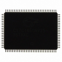
Manufacturer Part Number
CY7C1460AV25-167AXC
Description
SRAM (Static RAM)
Manufacturer
Cypress Semiconductor Corp
Datasheet
1.CY7C1460AV25-167BZC.pdf
(29 pages)
Specifications of CY7C1460AV25-167AXC
Format - Memory
RAM
Memory Type
SRAM - Synchronous
Memory Size
36M (1M x 36)
Speed
167MHz
Interface
Parallel
Voltage - Supply
2.375 V ~ 2.625 V
Operating Temperature
0°C ~ 70°C
Package / Case
100-LQFP
Lead Free Status / RoHS Status
Lead free / RoHS Compliant
Other names
428-2162
CY7C1460AV25-167AXC
CY7C1460AV25-167AXC
Available stocks
Company
Part Number
Manufacturer
Quantity
Price
Company:

Part Number:
CY7C1460AV25-167AXC
Manufacturer:
Cypress Semiconductor Corp
Quantity:
135
Company:
Part Number:
CY7C1460AV25-167AXC
Manufacturer:
MURATA
Quantity:
30 000
Company:
Part Number:
CY7C1460AV25-167AXC
Manufacturer:
Cypress Semiconductor Corp
Quantity:
10 000
Company:
Part Number:
CY7C1460AV25-167AXCT
Manufacturer:
Cypress Semiconductor Corp
Quantity:
10 000


Pin Configurations
Pin Definitions
Document Number: 38-05354 Rev. *G
Pin Name
BW
BW
BW
BW
BW
BW
BW
BW
WE
A0
A1
A
a
b
d
e
g
h
c
f
A
B
C
D
E
F
G
H
J
K
L
M
N
P
R
T
U
V
W
synchronous
synchronous
synchronous
I/O Type
Input-
Input-
Input-
DQPg
DQg
DQg
DQg
DQg
DQPd
DQc
NC
DQh
DQh
DQh
DQc
DQc
DQh
DQd
DQd
DQd
DQd
DQc
1
(continued)
DQg
DQg
DQg
DQg
DQPc
DQc
NC
DQh
DQh
DQh
DQPh
DQd
DQd
DQd
DQc
DQh
DQd
DQc
DQc
Address inputs used to select one of the address locations. Sampled at the rising edge of
the CLK.
Byte write select inputs, active LOW. Qualified with WE to conduct writes to the SRAM.
Sampled on the rising edge of CLK. BW
BW
controls DQ
Write enable input, active LOW. Sampled on the rising edge of CLK if CEN is active LOW. This
signal must be asserted LOW to initiate a write sequence.
2
c
controls DQ
209-ball FBGA (14 × 22 × 1.76 mm) Pinout
NC/144M
V
V
CLK
V
V
V
TMS
BWS
V
V
V
V
V
BWS
V
V
A
DDQ
DDQ
SS
SS
DDQ
SS
DDQ
SS
DDQ
SS
DDQ
A
SS
3
f
c
h
and DQP
CY7C1464AV25 (512 K × 72)
V
BWS
BWS
V
V
V
V
V
V
V
NC
NC
V
V
NC
CE
TDI
c
A
A
DDQ
DDQ
SS
SS
DDQ
SS
DDQ
DDQ
SS
DDQ
4
and DQP
2
g
d
f,
BW
NC/576M
NC/72M
NC/1G
V
V
V
V
V
V
V
V
NC
V
V
A
V
A
DD
A
NC
SS
DD
SS
SS
5
DD
DD
SS
g
DD
DD
SS
c
, BW
controls DQ
ADV/LD
d
CEN
MODE
NC
NC
CE
OE
NC
NC
NC
WE
NC
NC
V
V
ZZ
controls DQ
A1
A0
A
DD
DD
6
1
a
Pin Description
controls DQ
g
and DQP
V
V
NC
V
V
V
V
A
V
V
V
V
V
NC
A
A
NC
A
A
DD
SS
DD
DD
DD
7
SS
DD
SS
DD
SS
SS
d
and DQP
g,
V
V
BWS
V
V
BWS
V
V
V
a
V
V
V
TDO
CE
NC
NC
NC
SS
DDQ
A
BW
DDQ
SS
A
SS
DDQ
DDQ
SS
DDQ
and DQP
DDQ
8
3
b
e
h
d
, BW
controls DQ
NC/288M
BWS
V
V
V
V
V
V
V
BWS
V
V
V
V
V
TCK
NC
A
SS
SS
DDQ
DDQ
SS
DDQ
SS
SS
DDQ
SS
A
DDQ
DDQ
a
9
e
, BW
controls DQ
f
a
b
DQb
DQb
DQPf
DQb
DQb
DQPa
controls DQ
h
DQf
NC
DQa
DQa
DQa
DQf
DQf
DQa
DQe
DQe
DQe
DQe
DQf
and DQP
10
CY7C1460AV25
CY7C1462AV25
CY7C1464AV25
e
and DQP
DQb
DQb
DQb
DQb
DQPb
DQf
NC
DQa
DQa
DQa
DQPe
DQe
DQe
DQe
DQf
DQa
DQe
DQf
DQf
11
h
b
.
and DQP
Page 6 of 29
e,
BW
b
f
,
[+] Feedback
Related parts for CY7C1460AV25-167AXC
Image
Part Number
Description
Manufacturer
Datasheet
Request
R

Part Number:
Description:
Manufacturer:
Cypress Semiconductor Corp
Datasheet:
Part Number:
Description:
Manufacturer:
Cypress Semiconductor Corp
Datasheet:
Part Number:
Description:
Manufacturer:
Cypress Semiconductor Corp
Datasheet:
Part Number:
Description:
Manufacturer:
Cypress Semiconductor Corp
Datasheet:
Part Number:
Description:
Manufacturer:
Cypress Semiconductor Corp
Datasheet: