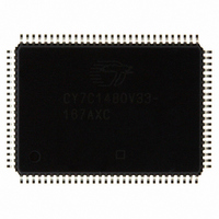
CY7C1480V33-167AXC Cypress Semiconductor Corp, CY7C1480V33-167AXC Datasheet - Page 14

CY7C1480V33-167AXC
Manufacturer Part Number
CY7C1480V33-167AXC
Description
CY7C1480V33-167AXC
Manufacturer
Cypress Semiconductor Corp
Datasheet
1.CY7C1480V33-167AXC.pdf
(31 pages)
Specifications of CY7C1480V33-167AXC
Format - Memory
RAM
Memory Type
SRAM - Synchronous
Memory Size
72M (2M x 36)
Speed
167MHz
Interface
Parallel
Voltage - Supply
3.135 V ~ 3.6 V
Operating Temperature
0°C ~ 70°C
Package / Case
100-LQFP
Density
72Mb
Access Time (max)
3.4ns
Sync/async
Synchronous
Architecture
SDR
Clock Freq (max)
167MHz
Operating Supply Voltage (typ)
3.3V
Address Bus
21b
Package Type
TQFP
Operating Temp Range
0C to 70C
Number Of Ports
4
Supply Current
450mA
Operating Supply Voltage (min)
3.135V
Operating Supply Voltage (max)
3.6V
Operating Temperature Classification
Commercial
Mounting
Surface Mount
Pin Count
100
Word Size
36b
Number Of Words
2M
Lead Free Status / RoHS Status
Lead free / RoHS Compliant
Lead Free Status / RoHS Status
Lead free / RoHS Compliant
Other names
428-2169
CY7C1480V33-167AXC
CY7C1480V33-167AXC
Available stocks
Company
Part Number
Manufacturer
Quantity
Price
Company:
Part Number:
CY7C1480V33-167AXC
Manufacturer:
CYPRESS
Quantity:
101
Company:
Part Number:
CY7C1480V33-167AXC
Manufacturer:
Cypress Semiconductor Corp
Quantity:
10 000
Company:
Part Number:
CY7C1480V33-167AXCT
Manufacturer:
Cypress Semiconductor Corp
Quantity:
10 000
Document Number: 38-05283 Rev. *J
The SRAM clock input might not be captured correctly if there
is no way in a design to stop (or slow) the clock during a
SAMPLE/PRELOAD instruction. If this is an issue, it is still
possible to capture all other signals and simply ignore the
value of the CLK captured in the boundary scan register.
After the data is captured, the data can be shifted out by
putting the TAP into the Shift-DR state. This places the
boundary scan register between the TDI and TDO balls.
Note that because the PRELOAD part of the command is not
implemented, putting the TAP to the Update-DR state while
performing a SAMPLE/PRELOAD instruction has the same
effect as the Pause-DR command.
TAP Timing
TAP AC Switching Characteristics
Clock
t
t
t
t
Output Times
t
t
Setup Times
t
t
t
Hold Times
t
t
t
Notes
Parameter
TCYC
TF
TH
TL
TDOV
TDOX
TMSS
TDIS
CS
TMSH
TDIH
CH
9. t
10. Test conditions are specified using the load in TAP AC Test Conditions. t
CS
and t
CH
refer to the setup and hold time requirements of latching data from the boundary scan register.
TCK Clock Cycle Time
TCK Clock Frequency
TCK Clock HIGH Time
TCK Clock LOW Time
TCK Clock LOW to TDO Valid
TCK Clock LOW to TDO Invalid
TMS Setup to TCK Clock Rise
TDI Setup to TCK Clock Rise
Capture Setup to TCK Rise
TMS Hold after TCK Clock Rise
TDI Hold after Clock Rise
Capture Hold after Clock Rise
Test M ode Select
Test Data-Out
Test Data-In
Test Clock
(TDO)
(TM S)
(TCK )
(TDI)
1
Description
Over the Operating Range
t TM SS
t TDIS
2
t TM SH
t TDIH
t TH
DON’T CA RE
R
/t
t
TL
F
= 1 ns.
3
BYPASS
When the BYPASS instruction is loaded in the instruction
register and the TAP is placed in a Shift-DR state, the bypass
register is placed between the TDI and TDO balls. The
advantage of the BYPASS instruction is that it shortens the
boundary scan path when multiple devices are connected
together on a board.
Reserved
These instructions are not implemented but are reserved for
future use. Do not use these instructions.
t CY C
[9, 10]
UNDEFINED
4
t TDOX
t TDOV
5
Min.
50
20
20
0
5
5
5
5
5
5
6
CY7C1480V33
CY7C1482V33
CY7C1486V33
Max.
20
10
Page 14 of 31
MHz
Unit
ns
ns
ns
ns
ns
ns
ns
ns
ns
ns
ns
[+] Feedback


