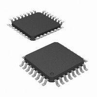
CY7C4211V-15AXI Cypress Semiconductor Corp, CY7C4211V-15AXI Datasheet - Page 5

CY7C4211V-15AXI
Manufacturer Part Number
CY7C4211V-15AXI
Description
IC,FIFO,512X9,SYNCHRONOUS,CMOS,TQFP,32PIN,PLASTIC
Manufacturer
Cypress Semiconductor Corp
Series
CY7Cr
Datasheet
1.CY7C4211V-15AI.pdf
(19 pages)
Specifications of CY7C4211V-15AXI
Function
Synchronous
Memory Size
4.6K (512 x 9)
Data Rate
100MHz
Access Time
10ns
Voltage - Supply
3.3V
Operating Temperature
-40°C ~ 85°C
Mounting Type
Surface Mount
Package / Case
32-TQFP
Lead Free Status / RoHS Status
Lead free / RoHS Compliant
Available stocks
Company
Part Number
Manufacturer
Quantity
Price
Company:
Part Number:
CY7C4211V-15AXI
Manufacturer:
Cypress Semiconductor Corp
Quantity:
10 000
Programming
When WEN2/LD is held LOW during Reset, this pin is the load
(LD) enable for flag offset programming. In this configuration,
WEN2/LD can be used to access the four 8-bit offset registers
contained in the CY7C42X1V for writing or reading data to these
registers.
When the device is configured for programmable flags and both
WEN2/LD and WEN1 are LOW, the first LOW-to-HIGH transition
of WCLK writes data from the data inputs to the empty offset
Least Significant Bit (LSB) register. The second, third, and fourth
LOW-to-HIGH transitions of WCLK store data in the empty offset
Most Significant Bit (MSB) register, full offset LSB register, and
full offset MSB register, respectively, when WEN2/LD and WEN1
are LOW. The fifth LOW-to-HIGH transition of WCLK while
Document #: 38-06010 Rev. *E
8
8
8
8
Figure 2. Offset Register Location and Default Values
256 x 9
Empty Offset (LSB) Reg.
Default Value = 007h
7
7
Full Offset (LSB) Reg
Default Value = 007h
0
0
0
0
8
8
8
8
WEN2/LD and WEN1 are LOW writes data to the empty LSB
register again.
values for the various device types.
It is not necessary to write to all the offset registers at one time.
A subset of the offset registers can be written; then by bringing
the WEN2/LD input HIGH, the FIFO is returned to normal read
and write operation. The next time WEN2/LD is brought LOW, a
write operation stores data in the next offset register in
sequence.
The contents of the offset registers can be read to the data
outputs when WEN2/LD is LOW and both REN1 and REN2 are
LOW. LOW-to-HIGH transitions of RCLK read register contents
to the data outputs. Writes and reads should not be performed
simultaneously on the offset registers.
512 x 9
Empty Offset (LSB) Reg.
Default Value = 007h
Full Offset (LSB) Reg
Default Value = 007h
7
7
(MSB)
Figure 2
(MSB)
0
0
0
0
0
0
shows the register sizes and default
CY7C4201V/4211V
Page 5 of 19
[+] Feedback


