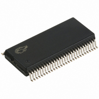
CY7C66113C-PVXCT Cypress Semiconductor Corp, CY7C66113C-PVXCT Datasheet - Page 30

CY7C66113C-PVXCT
Manufacturer Part Number
CY7C66113C-PVXCT
Description
IC,MICROCONTROLLER,8-BIT,SSOP,56PIN,PLASTIC
Manufacturer
Cypress Semiconductor Corp
Datasheet
1.CY7C66013C-PVXC.pdf
(59 pages)
Specifications of CY7C66113C-PVXCT
Applications
USB Hub/Microcontroller
Core Processor
M8
Program Memory Type
OTP (8 kB)
Controller Series
USB Hub
Ram Size
256 x 8
Interface
I²C, USB, HAPI
Number Of I /o
31
Voltage - Supply
4 V ~ 5.25 V
Operating Temperature
0°C ~ 70°C
Mounting Type
Surface Mount
Package / Case
56-SSOP
Processor Series
CY7C66xx
Core
M8
Data Bus Width
8 bit
Program Memory Size
8 KB
Data Ram Size
256 B
Interface Type
HAPI, I2C, USB
Maximum Clock Frequency
12 MHz
Number Of Programmable I/os
39
Number Of Timers
1
Maximum Operating Temperature
+ 70 C
Mounting Style
SMD/SMT
Development Tools By Supplier
CY3654, CY3654-P03
Minimum Operating Temperature
0 C
Lead Free Status / RoHS Status
Lead free / RoHS Compliant
For Use With
CY3649 - PROGRAMMER HI-LO USB M8428-1339 - KIT LOW SPEED PERSONALITY BOARD
Lead Free Status / Rohs Status
Details
DAC Interrupt
Each DAC I/O pin generates an interrupt, if enabled. The
interrupt polarity for each DAC I/O pin is programmable. A
positive polarity is a rising edge input while a negative polarity is
a falling edge input. All of the DAC pins share a single interrupt
vector, which means the firmware needs to read the DAC port to
determine which pin or pins caused an interrupt.
If one DAC pin has triggered an interrupt, no other DAC pins
causes a DAC interrupt until that pin has returned to its inactive
(non trigger) state or the corresponding interrupt enable bit is
cleared. The USB Controller does not assign interrupt priority to
different DAC pins and the DAC Interrupt Enable Register is not
cleared during the interrupt acknowledge process.
If one port pin has triggered an interrupt, no other port pins cause
a GPIO interrupt until that port pin has returned to its inactive
(non trigger) state or its corresponding port interrupt enable bit is
cleared. The USB Controller does not assign interrupt priority to
different port pins and the Port Interrupt Enable Registers are not
cleared during the interrupt acknowledge process.
When HAPI is enabled, the HAPI logic takes over the interrupt
vector and blocks any interrupt from the GPIO bits, including
ports and bits not used by HAPI. Operation of the HAPI interrupt
Document Number: 38-08024 Rev. *D
GPIO
Pin
IRA
1 = Enable
0 = Disable
Port Interrupt
Enable Register
Configuration
Register
M
U
X
Port
Figure 32. GPIO Interrupt Structure
1 = Enable
0 = Disable
(1 input per
OR Gate
GPIO pin)
(Bit 5, Register 0x20)
GPIO Interrupt
GPIO and HAPI Interrupt
Each of the GPIO pins generates an interrupt, if enabled. The
interrupt polarity is programmed for each GPIO port as part of
the GPIO configuration. All of the GPIO pins share a single
interrupt vector, which means the firmware needs to read the
GPIO ports with enabled interrupts to determine which pin or pins
caused an interrupt. A block diagram of the GPIO interrupt logic
is shown in
GPIO Interrupt Enable Ports
GPIO interrupt polarity and enabling individual GPIO interrupts.
is independent of the GPIO specific bit interrupt enables, and is
enabled or disabled only by bit 5 of the Global Interrupt Enable
Register (0x20) when HAPI is enabled. The settings of the GPIO
bit interrupt enables on ports and bits not used by HAPI still effect
the CMOS mode operation of those ports and bits. The effect of
modifying the interrupt bits while the Port Config bits are set to
‘10’ is shown in
interrupts are described in
(HAPI).
Global
Enable
1
GPIO Interrupt
Flip Flop
D
CLR
Figure
Q
CY7C66013C, CY7C66113C
Table
32. Refer to
6. The events that generate HAPI
Hardware Assisted Parallel Interface
for more information about setting
GPIO Configuration Port
Interrupt
Encoder
Priority
Page 30 of 59
Interrupt
IRQout
Vector
and
[+] Feedback


