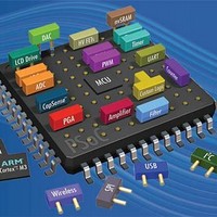
CY8C3865LTI-014 Cypress Semiconductor Corp, CY8C3865LTI-014 Datasheet
CY8C3865LTI-014
Specifications of CY8C3865LTI-014
Available stocks


Related parts for CY8C3865LTI-014


CY8C3865LTI-014 Summary of contents
Page 1
... AHB – AMBA (advanced microcontroller bus architecture) high-performance bus, an ARM data transfer bus 2. This feature on select devices only. See Ordering Information 3. GPIOs with opamp outputs are not recommended for use with CapSense. Cypress Semiconductor Corporation Document Number: 001-11729 Rev. *O PRELIMINARY ® ...
Page 2
Contents 1. Architectural Overview .........................................3 2. Pinouts ...................................................................5 3. Pin Descriptions ..................................................10 4. CPU .......................................................................11 4.1 8051 CPU .....................................................11 4.2 Addressing Modes ........................................11 4.3 Instruction Set ...............................................11 4.4 DMA and PHUB ............................................15 4.5 Interrupt Controller ........................................17 5. Memory .................................................................18 5.1 ...
Page 3
Architectural Overview Introducing the CY8C38 family of ultra low-power, flash Programmable System-on-Chip (PSoC PSoC 3 and 32-bit PSoC 5 platform. The CY8C38 family provides configurable blocks of analog, digital, and interconnect circuitry around a CPU subsystem. The combination of ...
Page 4
For more details on the peripherals see the Peripherals” section on page 35 of this datasheet. For information on UDBs, DSI, and other digital blocks, see the “Digital Subsystem” section on page 34 of this datasheet. PSoC’s analog subsystem is ...
Page 5
It also contains a separate, very low-power internal low-speed oscillator (ILO) for the sleep and watchdog timers. A 32.768-kHz external watch crystal is also supported for use in real-time clock (RTC) applications. The clocks, together with programmable clock dividers, provide ...
Page 6
P2[7] (GPIO, TMS, SWDIO) P1[0] (GPIO, TCK, SWDCK) P1[1] (GPIO, Configurable XRES) P1[2] (GPIO, TDO, SWV) P1[3] (GPIO, TDI) P1[4] (GPIO, nTRST) P1[5] Notes 7. Pins are No Connect (NC) on devices without USB. NC means that the pin ...
Page 7
P2[6] (GPIO) P2[7] (I2C0: SCL, SIO) P12[4] (I2C0: SDA, SIO) P12[5] Vboost XRES (TMS, SWDIO, GPIO) P1[0] (TCK, SWDCK, GPIO) P1[1] (configurable XRES, GPIO) P1[2] (TDO, SWV, GPIO) P1[3] (TDI, GPIO) P1[4] (nTRST, GPIO) P1[5] Vddio1 Notes 9. The ...
Page 8
P2[5] (GPIO) P2[6] (GPIO) P2[7] (I2C0: SCL, SIO) P12[4] (I2C0: SDA, SIO) P12[5] (GPIO) P6[4] (GPIO) P6[5] (GPIO) P6[6] (GPIO) P6[7] Vssb Ind Vboost Vbat Vssd XRES (GPIO) P5[0] (GPIO) P5[1] (GPIO) P5[2] (GPIO) P5[3] (TMS, SWDIO, GPIO) P1[0] ...
Page 9
Figure 2-5. Example Schematic for 100-pin TQFP Part with Power Connections Vddd C6 0.1 uF Vssd 1 P2[5] 2 P2[6] 3 P2[7] 4 P12[4], SIO 5 P12[5], SIO 6 P6[4] 7 P6[5] 8 P6[6] 9 P6[7] 10 Vssb 11 Ind ...
Page 10
Figure 2-6. Example PCB Layout for 100-pin TQFP Part for Optimal Analog Performance Vssd Plane 3. Pin Descriptions IDAC0, IDAC1, IDAC2, IDAC3 Low resistance output pin for high current DACs (IDAC). OpAmp0out, OpAmp1out, OpAmp2out, OpAmp3out High current output of uncommitted ...
Page 11
TMS JTAG test mode select programming and debug port connection. USBIO, D+ Provides D+ connection directly to a USB 2.0 bus. May be used as a digital I/O pin powered from V DDD Vddio. Pins are No Connect ...
Page 12
Instruction Set Summary 4.3.1.1 Arithmetic Instructions Arithmetic instructions support the direct, indirect, register, immediate constant, and register-specific instructions. Arithmetic modes are used for addition, subtraction, multiplication, division, increment, and decrement operations. instructions. Table 4-1. Arithmetic Instructions Mnemonic ADD A,Rn ...
Page 13
Table 4-2. Logical Instructions (continued) Mnemonic ANL Direct, #data AND immediate data to direct byte ORL A,Rn OR register to accumulator ORL A,Direct OR direct byte to accumulator ORL A,@Ri OR indirect RAM to accumulator ORL A,#data OR immediate data ...
Page 14
Table 4-3. Data Transfer Instructions (continued) Mnemonic MOV Direct, Direct Move direct byte to direct byte MOV Direct, @Ri Move indirect RAM to direct byte MOV Direct, #data Move immediate data to direct byte MOV @Ri, A Move accumulator to ...
Page 15
Program Branching Instructions The 8051 supports a set of conditional and unconditional jump instructions that help to modify the program execution flow. shows the list of jump instructions. Table 4-5. Jump Instructions Mnemonic ACALL addr11 Absolute subroutine call LCALL ...
Page 16
DMA Features 24 DMA channels Each channel has one or more transaction descriptors (TD) to configure channel behavior 128 total TDs can be defined TDs can be dynamically updated Eight levels of priority per ...
Page 17
Nested DMA One TD may modify another TD, as the TD configuration space is memory mapped similar to any other peripheral. For example, a first TD loads a second TD’s configuration and then calls the second TD. The second ...
Page 18
Memory 5.1 Static RAM CY8C38 SRAM is used for temporary data storage SRAM is provided and can be accessed by the 8051 or the DMA controller. See Memory Map on page 19. Simultaneous access ...
Page 19
Data, Address, and Control Signals PHUB Data, Address, and Control Signals Data, Address, and Control Signals 5.6 Memory Map The CY8C38 8051 memory map is very similar to the MCS-51 memory map. 5.6.1 Code Space The CY8C38 8051 code space ...
Page 20
In addition to the register or bit address modes used with the lower 48 bytes, the lower 128 bytes can be accessed with direct or indirect addressing. With direct addressing mode, the upper 128 bytes map to the SFRs. With ...
Page 21
Space The 8051 xdata space is 24-bit size. The majority of this space is not ‘external’—it is used by on-chip components. See Table 5-3. External, that is, off-chip, memory can be accessed using the ...
Page 22
MHz 4-33 MHz IMO ECO 12-48 MHz Doubler Digital Clock Divider 16 bit Digital Clock Divider 16 bit 7 Digital Clock Divider 16 bit Digital Clock Divider 16 bit 6.1.1 Internal Oscillators 6.1.1.1 Internal Main Oscillator In most designs ...
Page 23
The 33-kHz clock (CLK33K) comes from a divide-by-3 operation on CLK100K. This output can be used as a reduced accuracy version of the 32.768-kHz ECO clock with no need for a crystal. 6.1.2 External Oscillators 6.1.2.1 MHz External Crystal Oscillator ...
Page 24
Power System The power system consists of separate analog, digital, and I/O supply pins, labeled Vdda, Vddd, and Vddiox, respectively. It also includes two internal 1.8-V regulators that provide the digital (Vccd) and analog (Vcca) supplies for the internal ...
Page 25
Power Modes PSoC 3 devices have four different power modes, as shown in Table 6-2 and Table 6-3. The power modes allow a design to easily provide required functionality and processing power while simultaneously minimizing power consumption and maximizing ...
Page 26
Figure 6-5. Power Mode Transitions Active Manual Sleep Hibernate Buzz Alternate Active 6.2.1.1 Active Mode Active mode is the primary operating mode of the device. When in active mode, the active configuration template bits control which available resources are enabled ...
Page 27
The boost converter can be operated in two different modes: active and standby. Active mode is the normal mode of operation where the boost regulator actively generates a regulated output voltage. In standby mode, most boost functions are disabled, thus ...
Page 28
ALVI, DLVI, AHVI – Analog/digital low voltage interrupt, analog high voltage interrupt Interrupt circuits are available to detect when Vdda and Vddd go outside a voltage range. For AHVI, Vdda is compared to a fixed trip level. For ALVI ...
Page 29
Digital Input Path PRT[x]CTL PRT[x]DBL_SYNC_IN PRT[x]PS Digital System Input PICU[x]INTTYPE[y] PICU[x]INTSTAT Pin Interrupt Signal PICU[x]INTSTAT Digital Output Path PRT[x]SLW PRT[x]SYNC_OUT PRT[x]DR Digital System Output PRT[x]BYP PRT[x]DM2 PRT[x]DM1 PRT[x]DM0 Bidirectional Control PRT[x]BIE Analog Capsense Global Control CAPS[x]CFG1 PRT[x]AG Analog Global Enable ...
Page 30
Digital Input Path PRT[x]SIO_HYST_EN PRT[x]SIO_DIFF Reference Level PRT[x]DBL_SYNC_IN PRT[x]PS Digital System Input PICU[x]INTTYPE[y] PICU[x]INTSTAT Pin Interrupt Signal PICU[x]INTSTAT Digital Output Path Reference Level PRT[x]SIO_CFG PRT[x]SLW PRT[x]SYNC_OUT PRT[x]DR Digital System Output PRT[x]BYP PRT[x]DM2 PRT[x]DM1 PRT[x]DM0 Bidirectional Control PRT[x]BIE Digital Input Path ...
Page 31
Drive Modes Each GPIO and SIO pin is individually configurable into one of the eight drive modes listed in used for each pin (DM[2:0]) and set in the PRTxDM[2:0] registers. drive modes. Table 6-6 shows the I/O pin’s drive ...
Page 32
High impedance analog The default reset state with both the output driver and digital input buffer turned off. This prevents any current from flowing in the I/O’s digital input buffer due to a floating voltage. This state is recommended ...
Page 33
Analog Connections These connections apply only to GPIO pins. All GPIO pins may be used as analog inputs or outputs. The analog voltage present on the pin must not exceed the Vddio supply voltage to which the GPIO belongs. ...
Page 34
Over Voltage Tolerance All I/O pins provide an over voltage tolerance feature at any operating There are no current limitations for the SIO pins as they present a high impedance load to the external circuit ...
Page 35
Example Peripherals The flexibility of the CY8C38 family’s UDBs and analog blocks allow the user to create a wide range of components (peripherals). The most common peripherals were built and characterized by Cypress and are shown in the PSoC ...
Page 36
Component Catalog Figure 7-3. Component Catalog Document Number: 001-11729 Rev. *O PRELIMINARY ® PSoC 3: CY8C38 Family Datasheet Figure 7-2. PSoC Creator Framework The component catalog is a repository of reusable design elements that select device functionality and customize ...
Page 37
Software Development Figure 7-4. Code Editor Anchoring the tool is a modern, highly customizable user interface. It includes project management and integrated editors for C and assembler source code, as well the design entry tools. Project build control leverages ...
Page 38
The main component blocks of the UDB are: PLD blocks – There are two small PLDs per UDB. These blocks take inputs from the routing array and form registered or combinational sum-of-products logic. PLDs are used to implement state ...
Page 39
Datapath Module The datapath contains an 8-bit single cycle ALU, with associated compare and condition generation logic. This datapath block is optimized to implement embedded functions, such as timers, counters, integrators, PWMs, PRS, CRC, shifters and dead band generators ...
Page 40
Independent of the ALU operation, these functions are available: Shift left Shift right Nibble swap Bitwise OR mask 7.2.2.3 Conditionals Each datapath has two compares, with bit masking options. Compare operands include the two accumulators and ...
Page 41
Clock Generation Each subcomponent block of a UDB including the two PLDs, the datapath, and Status and Control, has a clock selection and control block. This promotes a fine granularity with respect to allocating clocking resources to UDB component ...
Page 42
Figure 7-13. Digital System Interconnect Timer Interrupt DMA CAN I2C Counters Controller Controller Digital System Routing I/F UDB ARRAY Digital System Routing I/F Global IO Port SC/CT EMIF Del-Sig Clocks Pins Blocks Interrupt and DMA routing is very flexible in ...
Page 43
CAN The CAN peripheral is a fully functional controller area network (CAN) supporting communication baud rates Mbps. The CAN controller implements the CAN2.0A and CAN2.0B specifications as defined in the Bosch specification and conforms to the ...
Page 44
Tx Buffer Status TxReq Pending TxInterrupt Request (if enabled) Acceptance Code 0 Rx Buffer RxMessage0 Status RxMessage RxMessage1 Acceptance Code 1 Available RxMessage14 Acceptance Code 14 RxInterrupt RxMessage15 Acceptance Code 15 Request (if enabled) 7.6 USB PSoC includes a dedicated ...
Page 45
Timers, Counters, and PWMs The timer/counter/PWM peripheral is a 16-bit dedicated peripheral providing three of the most common embedded peripheral features. As almost all embedded systems use some combination of timers, counters, and PWMs. Four of them have been ...
Page 46
Figure 7-22. DFB Application Diagram (pwr/gnd not shown) BUSCLK read_data write_data System addr Digital Digital Filter Routing Block DMA Request DMA CTRL The typical use model is for data to be supplied to the DFB over the system bus from ...
Page 47
The PSoC Creator software program provides a user friendly interface to configure the analog connections between the GPIO and various analog resources and connections from one analog resource to another. PSoC Creator also provides component libraries that allow you to ...
Page 48
ExVrefL ExVrefL1 opamp0 opamp2 swinp GPIO swfol swfol P0[4] swinn GPIO P0[5] GPIO * i0 abuf_vref_int P0[6] (1.024V) GPIO * i2 P0[7] cmp0_vref (1.024V) GPIO cmp_muxvn[1:0] P4[2] vref_cmp1 cmp1_vref (0.256V) GPIO bg_vda_res_en Vdda Vdda/2 ...
Page 49
Analog local buses (abus) are routing resources located within the analog subsystem and are used to route signals between different analog blocks. There are eight abus routes in CY8C38, four in the left half (abusl [0:3]) and four in the ...
Page 50
DMA controller or the CPU. 8.2.2.1 Single Sample In Single Sample mode, the ADC performs one sample conversion on a trigger. In this mode, the ADC stays ...
Page 51
From Analog Routing From Analog Routing 8.3.2 LUT The CY8C38 family of devices contains four LUTs. The LUT is a two input, one output lookup table that is driven by any one or two of the comparators in the chip. ...
Page 52
Figure 8-7. Opamp GPIO Analog Global Bus Opamp Analog Global Bus VREF Analog Internal Bus Analog Switch = GPIO The opamp is uncommitted and can be configured as a gain stage or voltage follower, or output buffer on external or ...
Page 53
Table 8-3. Bandwidth Gain Bandwidth 1 6.0 MHz 24 340 kHz 48 220 kHz 50 215 kHz Figure 8-9. PGA Resistor Settings ref 980 k ...
Page 54
Figure 8-11. LCD System LCD Global DAC Clock UDB LCD Driver Block Display DMA RAM PHUB 8.6.1 LCD Segment Pin Driver Each GPIO pin contains an LCD driver circuit. The LCD driver buffers the appropriate output of the LCD DAC ...
Page 55
Reference Source 8.9.1 Current DAC The current DAC (IDAC) can be configured for the ranges µ 256 µA, and 0 to 2.048 mA. The IDAC can be configured to source or sink current. 8.9.2 Voltage ...
Page 56
Down Mixer The SC/CT block can be used as a mixer to down convert an input signal. This circuit is a high bandwidth passive sample network that can sample input signals MHz. This sampled value is ...
Page 57
Debug Features Using the JTAG or SWD interface, the CY8C38 supports the following debug features: Halt and single-step the CPU View and change CPU and peripheral registers, and RAM addresses Eight program address breakpoints One memory ...
Page 58
Development Support The CY8C38 family has a rich set of documentation, development tools, and online resources to assist you during your development process. Visit psoc.cypress.com/getting-started to find out more. 10.1 Documentation A suite of documentation, supports the CY8C38 family ...
Page 59
Electrical Specifications Specifications are valid for –40 °C T 85 °C and T A except where noted. The unique flexibility of the PSoC UDBs and analog blocks enable many functions to be implemented in PSoC Creator components, ...
Page 60
Device Level Specifications Specifications are valid for –40 °C T 85 °C and T A except where noted. 11.2.1 Device Level Specifications Table 11-2. DC Specifications Parameter Description V Analog supply voltage and input to analog DDA ...
Page 61
Table 11-2. DC Specifications (continued) Parameter Description [20] Sleep Mode CPU = OFF RTC = ON (= ECO32K ON, in low-power mode) Sleep timer = ON (= ILO kHz) WDT = OFF Wake = ...
Page 62
Table 11-3. AC Specifications Parameter Description F CPU frequency CPU F Bus frequency BUSCLK Svdd V ramp rate DD T Time from IO_INIT DDD DDA IPOR to I/O ports set to their reset states T Time ...
Page 63
Power Regulators Specifications are valid for –40 °C T 85 °C and T A except where noted. 11.3.1 Digital Core Regulator Table 11-4. Digital Core Regulator DC Specifications Parameter Description V Input voltage DDD V Output voltage ...
Page 64
Table 11-6. Inductive Boost Regulator DC Specifications (continued) Parameter Description [26, 27] Boost output voltage range 1.8 V 1.9 V 2 BOOST 2.7 V 3.0 V 3.3 V 3.6 V 5.0 V Load regulation Line regulation ...
Page 65
Inputs and Outputs Specifications are valid for –40 °C T 85 °C and T A except where noted. 11.4.1 GPIO Table 11-8. GPIO DC Specifications Parameter Description V Input voltage high threshold IH V Input voltage low ...
Page 66
SIO Table 11-10. SIO DC Specifications Parameter Description Vinref Input voltage reference (Differential input mode) Output voltage reference (Regulated output mode) Voutref Input voltage high threshold GPIO mode V IH [29] Differential input mode Input voltage low threshold V ...
Page 67
Table 11-11. SIO AC Specifications (continued) Parameter Description SIO output operating frequency 3.3 V < V < 5.5 V, Unregulated DDIO output (GPIO) mode, fast strong drive mode 1.71 V < V < 3.3 V, DDIO Unregulated output (GPIO) mode, ...
Page 68
Table 11-13. USBIO AC Specifications Parameter Description Tdrate Full-speed data rate average bit rate Tjr1 Receiver data jitter tolerance to next transition Tjr2 Receiver data jitter tolerance to pair transition Tdj1 Driver differential jitter to next transition Tdj2 Driver differential ...
Page 69
Analog Peripherals Specifications are valid for –40 °C T 85 °C and T A except where noted. 11.5.1 Opamp Table 11-17. Opamp DC Specifications Parameter Description Vi Input voltage range Vioff Input offset voltage TCVos Input offset voltage drift ...
Page 70
Figure 11-2. Opamp Voffset Histogram, 60 samples / 15 parts, 25 °C, Vdda = 5V Figure 11-4. Opamp Voffset vs Common Mode Voltage and Temperature, Power Mode = High Document Number: 001-11729 Rev. *O PRELIMINARY ® PSoC 3: CY8C38 Family ...
Page 71
Figure 11-6. Opamp Operating Current vs Vdda, Power Mode = Minimum Figure 11-8. . Opamp Operating Current vs Vdda, Power Mode = Medium Document Number: 001-11729 Rev. *O PRELIMINARY ® PSoC 3: CY8C38 Family Datasheet Figure 11-7. Opamp Operating Current ...
Page 72
Table 11-18. Opamp AC Specifications Parameter Description GBW Gain-bandwidth product SR Slew Rate e Input noise density n Figure 11-10. Open Loop Gain and Phase vs Frequency and Temperature, Power Mode = High Pf, Vdda = 5V ...
Page 73
Figure 11-12. Opamp Closed Loop Frequency Response, Gain = 10, Vdda = 5V Figure 11-14. Opamp Noise vs Frequency, Power Mode = High, Vdda = 5V Figure 11-16. Opamp PSRR vs Frequency Document Number: 001-11729 Rev. *O PRELIMINARY ® PSoC ...
Page 74
Delta-sigma ADC Unless otherwise specified, operating conditions are: Operation in continuous sample mode fclk = 3.072 MHz for resolution = bits; fclk = 6.144 MHz for resolution = bits Reference = ...
Page 75
Table 11-19. 20-bit Delta-sigma ADC DC Specifications (continued) Parameter Description [35] Rin_ADC16 ADC input resistance [35] Rin_ADC12 ADC input resistance [35] Cin_G1 ADC input capacitance ADC external reference input voltage, see Vextref also internal reference in Voltage Reference on page ...
Page 76
Table 11-21. Delta-sigma ADC Sample Rates, Range = ±1.024 V Continuous Resolution, Bits Min Max 8 8000 384000 9 6400 307200 10 5566 267130 11 4741 227555 12 4000 192000 13 3283 157538 14 2783 133565 15 2371 113777 16 ...
Page 77
Figure 11-19. Delta-sigma ADC Noise Histogram, 1000 Samples, 20-Bit, 187 sps, Ext Ref ±1.024 V 100.00 90.00 80.00 70.00 60.00 50.00 40.00 30.00 20.00 10.00 0.00 ADC counts ADC Counts Figure 11-21. Delta-sigma ADC Noise Histogram, 1000 sam- ...
Page 78
Table 11-23. Delta-sigma ADC RMS Noise vs. Input Range and Sample Rate, 16-bit, Internal Reference RMS Noise, Counts Single-Ended Sample × 2 REF REF rate, sps 750 1500 3000 6000 12000 24000 48000 Figure ...
Page 79
Voltage Reference Table 11-24. Voltage Reference Specifications See also ADC external reference specifications in Section 11.5.2. Parameter Description V Precision reference voltage REF [38] Temperature drift Long term drift Thermal cycling drift (stability) 11.5.4 Analog Globals Table 11-25. Analog ...
Page 80
Table 11-27. Comparator AC Specifications Parameter Description Response time, high current [41] mode Response time, low current T [41] RESP mode Response time, ultra low-power [41] mode 11.5.6 Current Digital-to-analog Converter(IDAC) See the IDAC component datasheet in PSoC Creator for ...
Page 81
Table 11-28. IDAC DC Specifications (continued) Parameter Description I Operating current, code = 255 DD Figure 11-25. IDAC INL vs Input Code, Range = 255 µA, Source Mode Document Number: 001-11729 Rev. *O PRELIMINARY ® PSoC 3: CY8C38 Family Datasheet ...
Page 82
Figure 11-27. IDAC DNL vs Input Code, Range = 255 µA, Source Mode Figure 11-29. IDAC INL vs Temperature, Range = 255 µA, Fast Mode Figure 11-31. IDAC Full Scale Error vs Temperature, Range = 255 µA, Source Mode Document ...
Page 83
Figure 11-33. IDAC Operating Current vs Temperature, Range = 255 µA, Code = 0, Source Mode Table 11-29. IDAC AC Specifications Parameter Description F Update rate DAC T Settling time to 0.5 LSB SETTLE Document Number: 001-11729 Rev. *O PRELIMINARY ...
Page 84
Voltage Digital to Analog Converter (VDAC) See the VDAC component datasheet in PSoC Creator for full electrical specifications and APIs. Unless otherwise specified, all charts and graphs show typical values. Table 11-30. VDAC DC Specifications Parameter Description Resolution INL1 ...
Page 85
Figure 11-39. VDAC Full Scale Error vs Temperature Mode Figure 11-41. VDAC Operating Current vs Temperature, 1V Mode, Slow Mode Table 11-31. VDAC AC Specifications Parameter Description F Update rate DAC TsettleP Settling time to 0.1%, step 25% ...
Page 86
Mixer The mixer is created using a SC/CT analog block; see the Mixer component datasheet in PSoC Creator for full electrical specifications and APIs. Table 11-32. Mixer DC Specifications Parameter Description V Input offset voltage OS Quiescent current Table ...
Page 87
Transimpedance Amplifier The TIA is created using a SC/CT analog block; see the TIA component datasheet in PSoC Creator for full electrical specifications and APIs. Table 11-34. Transimpedance Amplifier (TIA) DC Specifications Parameter Description V Input offset voltage IOFF ...
Page 88
Programmable Gain Amplifier The PGA is created using a SC/CT analog block; see the PGA component datasheet in PSoC Creator for full electrical specifications and APIs. Unless otherwise specified, operating conditions are: Operating temperature = 25 °C for typical ...
Page 89
Table 11-37. PGA AC Specifications Parameter Description BW1 –3 dB bandwidth SR1 Slew rate e Input noise density n Figure 11-44. Gain vs. Frequency, at Different Gain Settings, Vdda = 3.3 V, Power Mode = High Figure 11-46. Noise vs. ...
Page 90
LCD Direct Drive Table 11-39. LCD Direct Drive DC Specifications Parameter Description I LCD operating current CC V LCD bias range (V refers to the BIAS BIAS main output voltage(V0) of LCD DAC) LCD bias step size LCD capacitance ...
Page 91
Digital Peripherals Specifications are valid for –40 °C T 85 °C and T A except where noted. 11.6.1 Timer The following specifications apply to the Timer/Counter/PWM peripheral in timer mode. Timers can also be implemented in UDBs; ...
Page 92
Pulse Width Modulation The following specifications apply to the Timer/Counter/PWM peripheral, in PWM mode. PWM components can also be implemented in UDBs; for more information, see the PWM component datasheet in PSoC Creator. Table 11-45. PWM DC Specifications Parameter ...
Page 93
Digital Filter Block Table 11-51. DFB DC Specifications Parameter Description DFB operating current Table 11-52. DFB AC Specifications Parameter Description F DFB operating frequency DFB 11.6.7 USB Table 11-53. USB DC Specifications Parameter Description V Device supply for USB ...
Page 94
Universal Digital Blocks (UDBs) PSoC Creator provides a library of prebuilt and tested standard digital peripherals (UART, SPI, LIN, PRS, CRC, timer, counter, PWM, AND, OR, and so on) that are mapped to the UDB array. See the component ...
Page 95
Memory Specifications are valid for –40 °C T 85 °C and T A except where noted. 11.7.1 Flash Table 11-55. Flash DC Specifications Parameter Description Erase and program voltage Table 11-56. Flash AC Specifications Parameter Description T ...
Page 96
SRAM Table 11-61. SRAM DC Specifications Parameter Description V SRAM retention voltage SRAM Table 11-62. SRAM AC Specifications Parameter Description F SRAM operating frequency SRAM 11.7.5 External Memory Interface Figure 11-48. Asynchronous Read Cycle Timing EM_ CEn Taddrv EM_ ...
Page 97
Table 11-63. Asynchronous Read Cycle Specifications Parameter Description [49] T EMIF clock period Tcel EM_CEn low time Taddrv EM_CEn low to EM_Addr valid Taddrh Address hold time after EM_Wen high Toel EM_OEn low time Tdoesu Data to EM_OEn high setup ...
Page 98
EM_ Clock EM_ CEn EM_ Addr EM_ OEn EM_ Data EM_ ADSCn Table 11-65. Synchronous Read Cycle Specifications Parameter Description [50] T EMIF clock period Tcp/2 EM_Clock pulse high Tceld EM_CEn low to EM_Clock high Tcehd EM_Clock high to EM_CEn ...
Page 99
EM_ Clock EM_ CEn EM_ Addr EM_ WEn EM_ Data EM_ ADSCn Table 11-66. Synchronous Write Cycle Specifications Parameter Description [51] T EMIF clock Period Tcp/2 EM_Clock pulse high Tceld EM_CEn low to EM_Clock high Tcehd EM_Clock high to EM_CEn ...
Page 100
PSoC System Resources Specifications are valid for –40 °C T 85 °C and T A except where noted. 11.8.1 POR with Brown Out For brown out detect in regulated mode, V mode. Table 11-67. Precise Power On ...
Page 101
Interrupt Controller Table 11-71. Interrupt Controller AC Specifications Parameter Description Delay from interrupt signal input to ISR code execution from ISR code 11.8.4 JTAG Interface Table 11-72. JTAG Interface AC Specifications Parameter Description f_TCK TCK frequency T_TDI_setup TDI setup ...
Page 102
Clocking Specifications are valid for –40 °C T 85 °C and T A except where noted. 11.9.1 32 kHz External Crystal Table 11-75. 32 kHz External Crystal DC Specifications Parameter Description I Operating current CC CL External ...
Page 103
Table 11-78. IMO AC Specifications (continued) Parameter Description [56] Jitter (peak to peak) Jp– MHz MHz [56] Jitter (long term) Jperiod MHz MHz 11.9.3 Internal Low-Speed Oscillator Table ...
Page 104
Phase-Locked Loop Table 11-83. PLL DC Specifications Parameter Description I PLL operating current DD Table 11-84. PLL AC Specifications Parameter Description [57] Fpllin PLL input frequency PLL intermediate frequency [57] Fpllout PLL output frequency Lock time at startup [59] ...
Page 105
... Del-Sig ✔ CY8C3865LTI-024 20-bit Del-Sig ✔ CY8C3865LTI-059 20-bit Del-Sig ✔ CY8C3865PVI-060 20-bit Del-Sig ✔ CY8C3865AXI-019 20-bit Del-Sig ✔ CY8C3865LTI-014 20-bit Del-Sig ✔ CY8C3865LTI-062 20-bit Del-Sig CY8C3865PVI-063 ✔ 20-bit Del-Sig 64 KB Flash CY8C3866AXI-054 – 20-bit Del-Sig CY8C3866LTI-020 – 20-bit Del-Sig ...
Page 106
Table 12-1. CY8C38 Family with Single Cycle 8051 (continued) MCU Core Part Number ✔ CY8C3866AXI-039 20-bit Del-Sig ✔ CY8C3866LTI-030 20-bit Del-Sig ✔ CY8C3866LTI-068 20-bit Del-Sig ✔ CY8C3866PVI-069 67 ...
Page 107
Part Numbering Conventions PSoC 3 devices follow the part numbering convention described here. All fields are single character alphanumeric ( … …, Z) unless stated otherwise. CY8Cabcdefg-xxx a: Architecture 3: PSoC 3 ...
Page 108
Packaging Table 13-1. Package Characteristics Parameter Description T Operating ambient temperature A T Operating junction temperature J Package JA (48-pin SSOP) Tja Package JA (48-pin QFN) Tja Package JA (68-pin QFN) Tja Package JA (100-pin TQFP) Tja Package JC ...
Page 109
TOP VIEW 7.00±0. PIN 1 DOT LASER MARK NOTES: 1. HATCH AREA IS SOLDERABLE EXPOSED METAL. 2. REFERENCE JEDEC#: MO-220 3. PACKAGE WEIGHT: 0.13g 4. ALL DIMENSIONS ARE IN MM [MIN/MAX] 5. PACKAGE CODE ...
Page 110
Figure 13-3. 68-pin QFN 8×8 with 0.4 mm Pitch Package Outline (Sawn Version) TOP VIEW 8.000±0.100 PIN 1 DOT LASER MARK NOTES: 1. HATCH AREA IS SOLDERABLE EXPOSED METAL. 2. REFERENCE JEDEC#: MO-220 ...
Page 111
Acronyms Table 14-1. Acronyms Used in this Document Acronym Description abus analog local bus ADC analog-to-digital converter AG analog global AHB AMBA (advanced microcontroller bus archi- tecture) high-performance bus, an ARM data transfer bus ALU arithmetic logic unit AMUXBUS ...
Page 112
Table 14-1. Acronyms Used in this Document (continued) Acronym Description PHUB peripheral hub PHY physical layer PICU port interrupt control unit PLA programmable logic array PLD programmable logic device, see also PAL PLL phase-locked loop PMDD package material declaration datasheet ...
Page 113
Table 16-1. Units of Measure (continued) Symbol Unit of Measure µF microfarads µH microhenrys µs microseconds µV microvolts µW microwatts mA milliamperes ms milliseconds mV millivolts nA nanoamperes ns nanoseconds nV nanovolts ohms pF picofarads ppm parts per million ...
Page 114
Revision History ® Description Title: PSoC 3: CY8C38 Family Datasheet Programmable System-on-Chip (PSoC Document Number: 001-11729 Submission Rev. ECN No. Date ** 571504 See ECN *A 754416 See ECN *B 2253366 See ECN *C 2350209 See ECN *D 2481747 ...
Page 115
Description Title: PSoC 3: CY8C38 Family Datasheet Programmable System-on-Chip (PSoC Document Number: 001-11729 *K 2903576 04/01/2010 Document Number: 001-11729 Rev. *O PRELIMINARY ® PSoC MKEA Updated Vb pin in PCB Schematic. Updated Tstartup parameter in AC Specifications table. Added ...
Page 116
Description Title: PSoC 3: CY8C38 Family Datasheet Programmable System-on-Chip (PSoC Document Number: 001-11729 *L 2938381 05/27/10 *M 2958674 06/22/10 *N 2989685 08/04/10 *O 3078568 11/04/10 Document Number: 001-11729 Rev. *O PRELIMINARY ® PSoC MKEA Replaced V with V in ...
Page 117
... Cypress against all charges. Any Source Code (software and/or firmware) is owned by Cypress Semiconductor Corporation (Cypress) and is protected by and subject to worldwide patent protection (United States and foreign), United States copyright laws and international treaty provisions. Cypress hereby grants to licensee a personal, non-exclusive, non-transferable license to copy, use, modify, create derivative works of, and compile the Cypress Source Code and derivative works for the sole purpose of creating custom software and or firmware in support of licensee product to be used only in conjunction with a Cypress integrated circuit as specified in the applicable agreement ...