DG4053AEQ-T1-E3 Vishay, DG4053AEQ-T1-E3 Datasheet - Page 6
DG4053AEQ-T1-E3
Manufacturer Part Number
DG4053AEQ-T1-E3
Description
Low Voltage AS/MUX
Manufacturer
Vishay
Datasheet
1.DG4051AEQ-T1-E3.pdf
(14 pages)
Specifications of DG4053AEQ-T1-E3
Function
Multiplexer
Circuit
3 x 2:1
On-state Resistance
100 Ohm
Voltage Supply Source
Single, Dual Supply
Voltage - Supply, Single/dual (±)
2.7 V ~ 12 V, ± 2.5 V ~ 5 V
Current - Supply
-1µA, 1µA
Operating Temperature
-40°C ~ 125°C
Mounting Type
Surface Mount
Package / Case
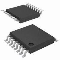
16-TSSOP
Number Of Channels
3 Channel
On Resistance (max)
265 Ohm @ 3 V
On Time (max)
151 ns @ 3 V
Off Time (max)
138 ns @ 3 V
Supply Voltage (max)
12 V
Supply Voltage (min)
2.7 V
Maximum Power Dissipation
450 mW
Maximum Operating Temperature
+ 125 C
Minimum Operating Temperature
- 40 C
Bandwidth
730 MHz
Mounting Style
SMD/SMT
Number Of Switches
Triple
Off Isolation (typ)
- 67 dB
Switch Current (typ)
0.00005 mA @ 5 V
Supply Current
0.05µA
On State Resistance Max
100ohm
Operating Temperature Range
-40°C To +125°C
Analogue Switch Case Style
TSSOP
No. Of Pins
16
Multiplexer Configuration
3 X 2
Svhc
No SVHC
Rohs Compliant
Yes
Supply Voltage Range
± 2.5V To ± 5V, 2.7V To 12V
Analog Switch Case Style
TSSOP
Lead Free Status / RoHS Status
Lead free / RoHS Compliant
Lead Free Status / RoHS Status
Lead free / RoHS Compliant
Other names
DG4053AEQ-T1-E3TR
Available stocks
Company
Part Number
Manufacturer
Quantity
Price
Company:

Part Number:
DG4053AEQ-T1-E3
Manufacturer:
LT
Quantity:
271
Part Number:
DG4053AEQ-T1-E3
Manufacturer:
VISHAY/威世
Quantity:
20 000


DG4051A, DG4052A, DG4053A
Vishay Siliconix
Notes:
a. V
b. Room = 25 °C, Full = as determined by the operating temperature suffix.
c. Typical values are for DESIGN AID ONLY, not guaranteed nor subject to production testing.
d. The algebraic convention whereby the most negative value is a minimum and the most positive a maximum, is used in this data sheet.
e. Guaranteed by design, not subject to production test.
Stresses beyond those listed under “Absolute Maximum Ratings” may cause permanent damage to the device. These are stress ratings only, and functional operation
of the device at these or any other conditions beyond those indicated in the operational sections of the specifications is not implied. Exposure to absolute maximum
rating conditions for extended periods may affect device reliability.
www.vishay.com
6
SPECIFICATIONS FOR UNIPOLAR SUPPLIES
Parameter
Analog Switch
Analog Signal Range
On-Resistance
Switch Off
Leakage Current
Channel On
Leakage Current
Digital Control
Input Current, V
Input Current, V
Dynamic Characteristics
Transition Time
Enable Turn-On Time
Enable Turn-Off Time
Break-Before-Make
Time Delay
Charge Injection
Off Isolation
Channel-to-Channel
Crosstalk
Source Off Capacitance
Drain Off Capacitance
Channel On
Capacitance
Power Supplies
Power Supply Current
Negative Supply Current
Ground Current
IN
= input voltage to perform proper function.
e
e
e
IN
IN
e
Low
High
e
e
e
V
Symbol
t
ANALOG
C
C
X
C
TRANS
OIRR
I
I
I
I
R
t
S(off)
D(off)
D(on)
t
GND
OFF
D(off)
D(on)
TALK
S(off)
I
ON
t
I+
I
Q
ON
I-
H
D
L
V
V
V
IN(A, B, C and ENABLE)
D
IN(A, B, C and ENABLE)
Unless Otherwise Specified
V
= 0.3 V/3.0 V, V
g
R
V
f = 1 MHz
f = 1 MHz
f = 1 MHz
= 0 V, R
V
I
V+ = + 3.3 V, V- = 0 V
V+ = + 3.3 V, V- = 0 V
V
V
R
S
CC
L
D
IN(A, B, C and ENABLE)
IN(A, B, C and ENABLE)
under test = 0.6 V
under test = 1.4 V
L
Test Conditions
= 300 , C
see figure 1, 2, 3
= 1 mA, V
= V
= 50 , C
= + 3 V, V
f = 100 kHz
S
g
= 0.3 V/3.0 V
= 0 , C
D
S
L
L
EE
= 1.5 V
= 1.4 V, 0.6 V
= 3.0 V/0.3 V
= 35 pF
= 1 pF
= 0 V or 3 V
= 0 V
L
DG4051A
DG4052A
DG4053A
DG4051A
DG4052A
DG4053A
DG4051A
DG4052A
DG4053A
= 1 nF
a
Temp.
Room
Room
Room
Room
Room
Room
Room
Room
Room
Room
Room
Room
Room
Room
Room
Room
Room
Room
Room
Room
Room
Room
Room
Full
Full
Full
Full
Full
Full
Full
Full
Full
Full
Full
Full
Full
Full
b
± 0.02
± 0.02
± 0.02
< - 90
< - 90
- 0.05
- 0.05
Typ.
0.01
0.01
0.05
175
0.5
81
71
69
14
19
14
11
4
3
4
8
5
c
- 40 °C to 125 °C - 40 °C to 85 °C
Min.
- 50
- 50
- 50
- 10
- 10
- 1
- 1
- 1
- 1
- 1
- 1
- 1
0
1
d
Max.
265
310
172
218
151
183
138
161
50
50
50
10
3
1
1
1
1
1
1
d
S10-1383-Rev. E, 21-Jun-10
Document Number: 69828
Min.
- 10
- 10
- 1
- 5
- 1
- 5
- 1
- 5
- 1
- 1
- 1
- 1
0
1
d
Max.
265
298
172
194
151
167
138
151
10
3
1
5
1
5
1
5
1
1
1
d
Unit
pC
nA
µA
dB
pF
µA
ns
V
Related parts for DG4053AEQ-T1-E3
Image
Part Number
Description
Manufacturer
Datasheet
Request
R

Part Number:
Description:
357-036-542-201 CARDEDGE 36POS DL .156 BLK LOPRO
Manufacturer:
Vishay
Datasheet:
Part Number:
Description:
357-036-542-201 CARDEDGE 36POS DL .156 BLK LOPRO
Manufacturer:
Vishay
Datasheet:
Part Number:
Description:
357-036-542-201 CARDEDGE 36POS DL .156 BLK LOPRO
Manufacturer:
Vishay
Datasheet:
Part Number:
Description:
357-036-542-201 CARDEDGE 36POS DL .156 BLK LOPRO
Manufacturer:
Vishay
Datasheet:
Part Number:
Description:
357-036-542-201 CARDEDGE 36POS DL .156 BLK LOPRO
Manufacturer:
Vishay
Datasheet:
Part Number:
Description:
357-036-542-201 CARDEDGE 36POS DL .156 BLK LOPRO
Manufacturer:
Vishay
Datasheet:
Part Number:
Description:
357-036-542-201 CARDEDGE 36POS DL .156 BLK LOPRO
Manufacturer:
Vishay
Datasheet:
Part Number:
Description:
357-036-542-201 CARDEDGE 36POS DL .156 BLK LOPRO
Manufacturer:
Vishay
Datasheet:
Part Number:
Description:
357-036-542-201 CARDEDGE 36POS DL .156 BLK LOPRO
Manufacturer:
Vishay
Datasheet:
Part Number:
Description:
357-036-542-201 CARDEDGE 36POS DL .156 BLK LOPRO
Manufacturer:
Vishay
Datasheet:
Part Number:
Description:
357-036-542-201 CARDEDGE 36POS DL .156 BLK LOPRO
Manufacturer:
Vishay
Datasheet:
Part Number:
Description:
357-036-542-201 CARDEDGE 36POS DL .156 BLK LOPRO
Manufacturer:
Vishay
Datasheet:
Part Number:
Description:
357-036-542-201 CARDEDGE 36POS DL .156 BLK LOPRO
Manufacturer:
Vishay
Datasheet:
Part Number:
Description:
357-036-542-201 CARDEDGE 36POS DL .156 BLK LOPRO
Manufacturer:
Vishay
Datasheet:
Part Number:
Description:
357-036-542-201 CARDEDGE 36POS DL .156 BLK LOPRO
Manufacturer:
Vishay
Datasheet: