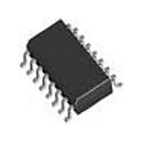
DS91M124TMA National Semiconductor, DS91M124TMA Datasheet

DS91M124TMA
Specifications of DS91M124TMA
Available stocks
Related parts for DS91M124TMA
DS91M124TMA Summary of contents
Page 1
... The DS91M124 has a flow-through pinout for easy PCB lay- out. It provides a new alternative for high speed multipoint interface applications packaged in a space saving SOIC-16 package. Typical Application © 2009 National Semiconductor Corporation DS91M124 Features ■ 125 MHz / 250 Mbps low jitter, low skew, low power operation ■ ...
Page 2
... Ordering Information Order Number DS91M124TMA Pin Diagram Logic Diagram Pin Descriptions Number Name GND 10, 11, 14 12, 13 N/C www.national.com Function 1:4 Repeater 30049801 30049803 I/O, Type I, LVCMOS Driver enable pin: When a DE pin is low, the corresponding driver output is disabled. When a DE pin is high, the corresponding driver output is enabled. There is a 300 kΩ ...
Page 3
... Absolute Maximum Ratings If Military/Aerospace specified devices are required, please contact the National Semiconductor Sales Office/ Distributors for availability and specifications. Power Supply Voltage LVCMOS Input Voltage M-LVDS Output Voltage M-LVDS Output Short Circuit Current Duration Junction Temperature Storage Temperature Range Lead Temperature Range Soldering (4 sec.) Maximum Package Power Dissipation @ +25° ...
Page 4
Symbol Parameter I Driver High-Impedance Output Power-Off Current A(OFF) I Driver High-Impedance Output Power-Off Current B(OFF) I Driver High-Impedance Output Power-Off Current AB(OFF) (I − A(OFF) B(OFF) C Driver Output Capacitance A C Driver Output Capacitance B C ...
Page 5
Switching Characteristics Over supply voltage and operating temperature ranges, unless otherwise specified. Symbol t Differential Propagation Delay High to Low PHL t Differential Propagation Delay Low to High PLH t Differential Pulse Skew |t SKD1 t Channel-to-Channel Skew SKD2 t ...
Page 6
Test Circuits and Waveforms www.national.com FIGURE 1. Differential Driver Test Circuit FIGURE 2. Differential Driver Waveforms FIGURE 3. Differential Driver Full Load Test Circuit 6 30049814 30049844 30049822 ...
Page 7
FIGURE 4. Differential Driver DC Open Test Circuit FIGURE 5. Differential Driver Short-Circuit Test Circuit FIGURE 6. Driver Propagation Delay and Transition Time Test Circuit 7 30049812 30049825 30049816 www.national.com ...
Page 8
FIGURE 7. Driver Propagation Delays and Transition Time Waveforms www.national.com FIGURE 8. Driver TRI-STATE Delay Test Circuit FIGURE 9. Driver TRI-STATE Delay Waveforms 8 30049818 30049819 30049821 ...
Page 9
Typical Performance Characteristics Driver Rise Time as a Function of Temperature Driver Fall Time as a Function of Temperature Driver Output Signal Amplitude as a Function of Resistive Load 30049850 Driver Propagation Delay (tPLHD Function of 30049851 Driver ...
Page 10
... Physical Dimensions 16-Lead (0.150 Wide) Molded Small Outline Package, JEDEC www.national.com inches (millimeters) unless otherwise noted Order Number DS91M124TMA NS Package Number M16A 10 ...
Page 11
Notes 11 www.national.com ...
Page 12
... For more National Semiconductor product information and proven design tools, visit the following Web sites at: Products Amplifiers www.national.com/amplifiers Audio www.national.com/audio Clock and Timing www.national.com/timing Data Converters www.national.com/adc Interface www.national.com/interface LVDS www.national.com/lvds Power Management www.national.com/power Switching Regulators www.national.com/switchers LDOs www.national.com/ldo LED Lighting www ...


