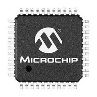
DSPIC33FJ128GP804-H/PT Microchip Technology, DSPIC33FJ128GP804-H/PT Datasheet - Page 264

DSPIC33FJ128GP804-H/PT
Manufacturer Part Number
DSPIC33FJ128GP804-H/PT
Description
16-bit DSC, 128KB Flash, CAN, DMA, 40 MIPS, NanoWatt 44 TQFP 10x10x1mm TRAY
Manufacturer
Microchip Technology
Series
dsPIC™ 33Fr
Datasheet
1.DSPIC33FJ32GP302-ISO.pdf
(412 pages)
Specifications of DSPIC33FJ128GP804-H/PT
Core Processor
dsPIC
Core Size
16-Bit
Speed
40 MIPs
Connectivity
CAN, I²C, IrDA, LIN, SPI, UART/USART
Peripherals
AC'97, Brown-out Detect/Reset, DMA, I²S, POR, PWM, WDT
Number Of I /o
35
Program Memory Size
128KB (128K x 8)
Program Memory Type
FLASH
Ram Size
16K x 8
Voltage - Supply (vcc/vdd)
3 V ~ 3.6 V
Data Converters
A/D 13x10b/12b, D/A 6x16b
Oscillator Type
Internal
Operating Temperature
-40°C ~ 140°C
Package / Case
44-TQFP
Processor Series
dsPIC33F
Core
dsPIC
Data Bus Width
16 bit
Interface Type
SPI, I2C, UART, JTAG
Number Of Programmable I/os
35
Operating Supply Voltage
3.3 V
Maximum Operating Temperature
+ 140 C
Mounting Style
SMD/SMT
Development Tools By Supplier
MPLAB IDE Software
Minimum Operating Temperature
- 40 C
On-chip Adc
10 bit, 13 Channel
A/d Bit Size
10 bit
A/d Channels Available
13
Lead Free Status / RoHS Status
Lead free / RoHS Compliant
Eeprom Size
-
Lead Free Status / Rohs Status
Details
Available stocks
Company
Part Number
Manufacturer
Quantity
Price
Company:
Part Number:
DSPIC33FJ128GP804-H/PT
Manufacturer:
Microchip Technology
Quantity:
10 000
- Current page: 264 of 412
- Download datasheet (6Mb)
dsPIC33FJ32GP302/304, dsPIC33FJ64GPX02/X04, AND dsPIC33FJ128GPX02/X04
REGISTER 21-7:
REGISTER 21-8:
DS70292E-page 264
bit 15
bit 7
Legend:
R = Readable bit
-n = Value at POR
bit 15-12
bit 11-0
Note 1:
bit 15
bit 7
Legend:
R = Readable bit
-n = Value at POR
bit 15-13
bit 12-0
Note 1:
PCFG7
R/W-0
R/W-0
CSS7
U-0
U-0
—
—
2:
2:
3:
On devices without 13 analog inputs, all AD1CSSL bits can be selected by the user application. However,
inputs selected for scan without a corresponding input on device converts V
CSSx = ANx, where x = 0 through 12.
On devices without 13 analog inputs, all PCFG bits are R/W by user software. However, the PCFG bits are
ignored on ports without a corresponding input on device.
PCFGx = ANx, where x = 0 through 12.
PCFGx bits have no effect if ADC module is disabled by setting ADxMD bit in the PMDx Register. In this
case all port pins multiplexed with ANx will be in Digital mode.
Unimplemented: Read as ‘0’
CSS<11:0>: ADC Input Scan Selection bits
1 = Select ANx for input scan
0 = Skip ANx for input scan
Unimplemented: Read as ‘0’
PCFG<12:0>: ADC Port Configuration Control bits
1 = Port pin in Digital mode, port read input enabled, ADC input multiplexor connected to AV
0 = Port pin in Analog mode, port read input disabled, ADC samples pin voltage
PCFG6
R/W-0
R/W-0
CSS6
U-0
U-0
—
—
AD1CSSL: ADC1 INPUT SCAN SELECT REGISTER LOW
AD1PCFGL: ADC1 PORT CONFIGURATION REGISTER LOW
W = Writable bit
‘1’ = Bit is set
W = Writable bit
‘1’ = Bit is set
PCFG5
R/W-0
R/W-0
CSS5
U-0
U-0
—
—
PCFG12
PCFG4
CSS12
R/W-0
R/W-0
R/W-0
R/W-0
CSS4
U = Unimplemented bit, read as ‘0’
U = Unimplemented bit, read as ‘0’
‘0’ = Bit is cleared
‘0’ = Bit is cleared
PCFG11
PCFG3
CSS11
R/W-0
R/W-0
R/W-0
R/W-0
CSS3
PCFG10
PCFG2
CSS10
R/W-0
R/W-0
R/W-0
R/W-0
CSS2
REFL
© 2011 Microchip Technology Inc.
(1,2)
x = Bit is unknown
x = Bit is unknown
.
PCFG9
PCFG1
R/W-0
R/W-0
R/W-0
R/W-0
CSS9
CSS1
(1,2,3)
PCFG8
PCFG0
R/W-0
R/W-0
R/W-0
R/W-0
CSS8
CSS0
SS
bit 8
bit 0
bit 8
bit 0
Related parts for DSPIC33FJ128GP804-H/PT
Image
Part Number
Description
Manufacturer
Datasheet
Request
R

Part Number:
Description:
Manufacturer:
Microchip Technology Inc.
Datasheet:

Part Number:
Description:
Manufacturer:
Microchip Technology Inc.
Datasheet:

Part Number:
Description:
Manufacturer:
Microchip Technology Inc.
Datasheet:

Part Number:
Description:
Manufacturer:
Microchip Technology Inc.
Datasheet:

Part Number:
Description:
Manufacturer:
Microchip Technology Inc.
Datasheet:

Part Number:
Description:
Manufacturer:
Microchip Technology Inc.
Datasheet:

Part Number:
Description:
Manufacturer:
Microchip Technology Inc.
Datasheet:

Part Number:
Description:
Manufacturer:
Microchip Technology Inc.
Datasheet:


