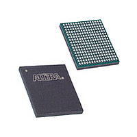
EPM7512BFC256-10 Altera, EPM7512BFC256-10 Datasheet - Page 19

EPM7512BFC256-10
Manufacturer Part Number
EPM7512BFC256-10
Description
MAX 7000/S/AE/B
Manufacturer
Altera
Datasheet
1.EPM7512BFC256-10.pdf
(66 pages)
Specifications of EPM7512BFC256-10
Family Name
MAX 7000B
Memory Type
EEPROM
# Macrocells
512
Number Of Usable Gates
10000
Frequency (max)
125MHz
Propagation Delay Time
10ns
Number Of Logic Blocks/elements
32
# I/os (max)
212
Operating Supply Voltage (typ)
2.5V
In System Programmable
Yes
Operating Supply Voltage (min)
2.375V
Operating Supply Voltage (max)
2.625V
Operating Temp Range
0C to 70C
Operating Temperature Classification
Commercial
Mounting
Surface Mount
Pin Count
256
Package Type
FBGA
Lead Free Status / Rohs Status
Not Compliant
Available stocks
Company
Part Number
Manufacturer
Quantity
Price
Programming
with External
Hardware
IEEE Std.
1149.1 (JTAG)
Boundary-Scan
Support
Altera Corporation
SAMPLE/PRELOAD
EXTEST
BYPASS
CLAMP
IDCODE
USERCODE
ISP Instructions
Table 6. MAX 7000B JTAG Instructions
JTAG Instruction
f
Allows a snapshot of signals at the device pins to be captured and examined during
normal device operation, and permits an initial data pattern output at the device pins.
Allows the external circuitry and board-level interconnections to be tested by forcing a
test pattern at the output pins and capturing test results at the input pins.
Places the 1-bit bypass register between the TDI and TDO pins, which allows the
boundary-scan test data to pass synchronously through a selected device to adjacent
devices during normal operation.
Allows the values in the boundary-scan register to determine pin states while placing the
1-bit bypass register between the TDI and TDO pins.
Selects the IDCODE register and places it between the TDI and TDO pins, allowing the
IDCODE to be serially shifted out of TDO.
Selects the 32-bit USERCODE register and places it between the TDI and TDO pins,
allowing the USERCODE value to be shifted out of TDO.
These instructions are used when programming MAX 7000B devices via the JTAG ports
with the MasterBlaster or ByteBlasterMV download cable, or using a Jam File (.jam),
Jam Byte-Code File (.jbc), or Serial Vector Format File (.svf) via an embedded
processor or test equipment.
MAX 7000B devices can be programmed on Windows-based PCs with an
Altera Logic Programmer card, the Master Programming Unit (MPU),
and the appropriate device adapter. The MPU performs continuity
checking to ensure adequate electrical contact between the adapter and
the device.
For more information, see the
The Altera software can use text- or waveform-format test vectors created
with the Altera Text Editor or Waveform Editor to test the programmed
device. For added design verification, designers can perform functional
testing to compare the functional device behavior with the results of
simulation.
Data I/O, BP Microsystems, and other programming hardware
manufacturers provide programming support for Altera devices. For
more information, see
MAX 7000B devices include the JTAG boundary-scan test circuitry
defined by IEEE Std. 1149.1.
supported by MAX 7000B devices. The pin-out tables starting on
of this data sheet show the location of the JTAG control pins for each
device. If the JTAG interface is not required, the JTAG pins are available
as user I/O pins.
Programming Hardware
MAX 7000B Programmable Logic Device Data Sheet
Description
Table 6
Altera Programming Hardware Data
describes the JTAG instructions
Manufacturers.
Sheet.
page 59
19


