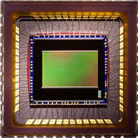
MT9V032C12STC Aptina LLC, MT9V032C12STC Datasheet - Page 5

MT9V032C12STC
Manufacturer Part Number
MT9V032C12STC
Description
SENSOR IMAGE VGA COLOR 48LCC
Manufacturer
Aptina LLC
Series
DigitalClarity®, Micron®r
Type
CMOS Imagingr
Datasheet
1.MT9V032C12STM.pdf
(13 pages)
Specifications of MT9V032C12STC
Pixel Size
6µm x 6µm
Active Pixel Array
752H x 480V
Frames Per Second
60
Voltage - Supply
3.3V
Package / Case
48-CLCC
Lead Free Status / RoHS Status
Lead free / RoHS Compliant
Other names
557-1237
MT9V032C12STC ES
Q3986409
MT9V032C12STC ES
Q3986409
Table 3:
PDF: 09005aef824c9998/Source: 09005aef824c999c
MT9V032_LDS_2.fm - Rev. B 3/07 EN
Pin Number
29
10
11
23
25
28
30
31
32
33
47
24
22
26
20
21
15
16
17
18
19
27
41
42
43
44
45
46
8
9
2
3
4
5
Pin Descriptions
Only pins D
BYPASS_CLKIN_N
SER_DATAOUT_N
BYPASS_CLKIN_P
SHFT_CLKOUT_N
SER_DATAOUT_P
SHFT_CLKOUT_P
SER_DATAIN_N
SER_DATAIN_P
FRAME_VALID
S_CTRL_ADR0
S_CTRL_ADR1
STFRM_OUT
LINE_VALID
EXPOSURE
STLN_OUT
STANDBY
LED_OUT
Symbol
SYSCLK
RESET#
PIXCLK
D
D
D
D
D
D
D
D
D
D
S
RSVD
SCLK
DATA
OUT
OUT
OUT
OUT
OUT
OUT
OUT
OUT
OUT
OUT
OE
OUT
5
6
7
8
9
4
3
2
1
0
0 through D
OUT
Output
Output
Output
Output
Output
Output
Output
Output
Output
Output
Output
Output
Output
Output
Output
Output
Output
Output
Input
Input
Input
Input
Input
Input
Input
Input
Input
Input
Input
Input
Input
Type
9 may be tri-stated
I/O
I/O
I/O
MT9V032: 1/3-Inch Wide-VGA Digital Image Sensor
Connect to D
Serial data in for stereoscopy (differential negative). Tie to
1kΩ pull-up (to 3.3V) in non-stereoscopy mode.
Serial data in for stereoscopy (differential positive). Tie to
D
Input bypass shift-CLK (differential negative). Tie to 1KΩ
pull-up (to 3.3V) in non-stereoscopy mode.
Input bypass shift-CLK (differential positive). Tie to D
in non-stereoscopy mode.
Rising edge starts exposure in slave mode.
Two-wire serial interface clock. Connect to V
resistor even when no other two-wire serial interface
peripheral is attached.
D
Two-wire serial interface slave address bit 3.
Two-wire serial interface slave address bit 5.
Asynchronous reset. All registers assume defaults.
Shut down sensor operation for power saving.
Master clock (26.6 MHz).
Two-wire serial interface data. Connect to V
resistor even when no other two-wire serial interface
peripheral is attached.
Output in master mode
in-phase; input in slave mode.
Output in master mode
chip in-phase; input in slave mode.
Asserted when D
Asserted when D
Parallel pixel data output 5.
Parallel pixel data output 6.
Parallel pixel data output 7.
Parallel pixel data output 8
Parallel pixel data output 9.
LED strobe output.
Parallel pixel data output 4.
Parallel pixel data output 3.
Parallel pixel data output 2.
Parallel pixel data output 1.
Parallel pixel data output 0.
Pixel clock out. D
Output shift CLK (differential negative).
Output shift CLK (differential positive).
Serial data out (differential negative).
Serial data out (differential positive).
GND
OUT
5
enable pad, active HIGH.
in non-stereoscopy mode.
GND
Micron Technology, Inc., reserves the right to change products or specifications without notice.
.
OUT
OUT
OUT
data is valid.
data is valid.
is valid on rising edge of this clock.
Description
—
—
start line sync to drive slave chip
start frame sync to drive a slave
©2006 Micron Technology, Inc. All rights reserved.
DD
DD
Pin Descriptions
with 1.5K
with 1.5K
GND
Preliminary
Notes
1
2
‡


