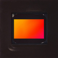
MT9V022I77ATC Aptina LLC, MT9V022I77ATC Datasheet - Page 50

MT9V022I77ATC
Manufacturer Part Number
MT9V022I77ATC
Description
IC SENSOR IMAGE VGA COLOR 52IBGA
Manufacturer
Aptina LLC
Type
CMOS Imagingr
Series
DigitalClarity®r
Specifications of MT9V022I77ATC
Pixel Size
6µm x 6µm
Active Pixel Array
752H x 480V
Frames Per Second
60
Voltage - Supply
3.3V
Package / Case
52-IBGA
Sensor Image Color Type
Color
Sensor Image Size Range
250,920 to 480,000Pixels
Sensor Image Size
752x480Pixels
Operating Supply Voltage (min)
3V
Operating Supply Voltage (typ)
3.3V
Operating Supply Voltage (max)
3.6V
Operating Temp Range
-40C to 85C
Package Type
IBGA
Operating Temperature Classification
Industrial
Mounting
Surface Mount
Pin Count
52
Lead Free Status / RoHS Status
Lead free / RoHS Compliant
Other names
557-1267
MT9V022I77ATC
MT9V022I77ATC
Configuration of Sensor for Stereoscopic Serial Output with Internal PLL
Figure 47:
PDF: 3295348826/Source:7478516499
MT9V022_DS - Rev.H 6/10 EN
Stereoscopic Topology
Note:
10. Individual WRITE to slave sensor, setting it as a stereo slave (set R0x07[6] = 1).
11. Individual WRITEs to master sensor to minimize the inter-sensor skew (set
12. Broadcast WRITE to issue a soft reset (set R0x0C[0] = 1 followed by R0x0C[0] = 0).
1. Power up the sensors.
2. Broadcast WRITE to de-assert LVDS power-down (set R0xB1[1] = 0).
3. Individual WRITE to master sensor putting its internal PLL into bypass mode (set
4. Broadcast WRITE to both sensors to set the stereoscopy bit (set R0x07[5] = 1).
5. Make sure all resolution, vertical blanking, horizontal blanking, window size, and
6. Broadcast WRITE to enable LVDS driver (set R0xB3[4] = 0).
7. Broadcast WRITE to enable LVDS receiver (set R0xB2[4] = 0).
8. Individual WRITE to master sensor, putting its internal PLL into bypass mode (set
9. Individual WRITE to slave sensor, enabling its internal PLL (set R0xB1[0] = 0).
In this configuration the internal PLL generates the shift-clk (x18) in phase with the
system-clock. The LVDS pins SER_DATAOUT_P and SER_DATAOUT_N must be
connected to a deserializer (clocked at approximately the same system clock frequency).
Figure 47 shows how a standard off-the-shelf deserializer can be used to retrieve back
D
out LINE_VALID and FRAME_VALID embedded within the pixel data stream.
Typical configuration of the master and slave sensors:
BYPASS_CLKIN
SER_DATAIN
OUT
R0xB1[0] = 1).
AEC/AGC configurations are done through broadcast WRITE to maintain lockstep.
R0xB1[0] = 1).
R0xB2[2:0], R0xB3[2:0], and R0xB4[1:0] appropriately). Use R0xB7 and R0xB8 to get
lockstep feedback from stereo_error_flag.
The stereo_error_flag is set if a mismatch has occurred at a reserved byte (slave and
master sensor’s codes at this reserved byte must match). If the flag is set, steps 11 and
12 are repeated until the stereo_error_flag remains cleared.
LVDS
LVDS
(9:2) for both the master and slave sensors. Additional logic is required to extract
1. PLL in non-bypass mode
2. PLL in x 18 mode (stereoscopy)
X 1 8/X 1 2 PL L
SENSOR
SENSOR
SLAVE
SER_DATAOUT
LVDS
SHIFT_CLKOUT
LVDS
50
1. PLL in bypass mode
BYPASS_CLKIN
SER_DATAIN
MT9V022: 1/3-Inch Wide-VGA Digital Image Sensor
LVDS
LVDS
MASTER
SENSOR
LV and FV are embedded in the data stream
SER_DATAOUT
FROM
SLAVE
PIXEL
8
LVDS
DS92LV16
Appendix A – Serial Configurations
Aptina reserves the right to change products or specifications without notice.
LVDS
SHIFT_CLKOUT
MASTER
PIXEL
FROM
8
26.6 MHz
26.6 MHz
©2005 Aptina Imaging Corporation. All rights reserved.
Osc.
Osc.
5 meters (maximum)


