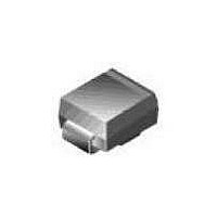
MBRS410LT3
Surface Mount
Schottky Power Rectifier
metal−to−silicon power diode. State−of−the−art geometry features
epitaxial construction with oxide passivation and metal overlay
contact. Ideally suited for low voltage, high frequency rectification, or
as free wheeling and polarity protection diodes, in surface mount
applications where compact size and weight are critical to the system.
Typical applications are AC−DC and DC−DC converters, reverse
battery protection, and “ORing” of multiple supply voltages and any
other application where performance and size are critical.
Features
•
•
•
•
•
•
•
•
•
Mechanical Characteristics
•
•
•
•
•
•
Maximum ratings are those values beyond which device damage can occur.
Maximum ratings applied to the device are individual stress limit values (not
normal operating conditions) and are not valid simultaneously. If these limits are
exceeded, device functional operation is not implied, damage may occur and
reliability may be affected.
MAXIMUM RATINGS
© Semiconductor Components Industries, LLC, 2005
August, 2005 − Rev. 2
Peak Repetitive Reverse Voltage
Average Rectified Forward Current
Non−Repetitive Peak Surge Current
Operating Junction Temperature
This device employs the Schottky Barrier principle in a large area
Leads are Readily Solderable
260°C Max. for 10 Seconds
Ultra Low V
1st in the Market Place with a 10 V
Small Compact Surface Mountable Package with J−Bend Leads
Rectangular Package for Automated Handling
Highly Stable Oxide Passivated Junction
Very Low Forward Voltage Drop
Excellent Ability to Withstand Reverse Avalanche Energy Transients
Guard−Ring for Stress Protection
Pb−Free Package is Available
Case: Epoxy, Molded
Weight: 217 mg (Approximately)
Finish: All External Surfaces Corrosion Resistant and Terminal
Lead and Mounting Surface Temperature for Soldering Purposes:
Polarity: Notch in Plastic Body Indicates Cathode Lead
ESD Ratings:
Working Peak Reverse Voltage
DC Blocking Voltage
(@ T
(Surge Applied at Rated Load Conditions
Halfwave, Single Phase, 60 Hz)
L
= 110°C)
F
Rating
Machine Model = C
Human Body Model = 3B
Preferred Device
R
Schottky Rectifier
Symbol
V
V
I
RWM
FSM
RRM
V
T
I
O
R
J
−65 to +125
Value
150
4.0
10
1
Unit
°C
V
A
A
MBRS410LT3G
†For information on tape and reel specifications,
Preferred devices are recommended choices for future use
and best overall value.
MBRS410LT3
including part orientation and tape sizes, please
refer to our Tape and Reel Packaging Specification
Brochure, BRD8011/D.
Device
4.0 AMPERES, 10 VOLTS
SCHOTTKY BARRIER
ORDERING INFORMATION
B4L1
A
Y
WW
G
(Note: Microdot may be in either location)
MARKING DIAGRAM
http://onsemi.com
RECTIFIERS
(Pb−Free)
= Specific Device Code
= Assembly Location
= Year
= Work Week
= Pb−Free Package
Package
CASE 403
PLASTIC
SMC
SMC
AYWW
SMC
B4L1G
Publication Order Number:
G
2500/Tape & Reel
2500/Tape & Reel
MBRS410LT3/D
Shipping
†


