MBD110DWT1G ON Semiconductor, MBD110DWT1G Datasheet
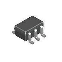
Schottky (Diodes & Rectifiers) 7V 120mW Dual Isolated

MBD110DWT1G

Manufacturer Part Number
MBD110DWT1G
Description
Schottky (Diodes & Rectifiers) 7V 120mW Dual Isolated
Manufacturer
ON Semiconductor
Series
-r
Datasheet

Specifications of MBD110DWT1G

Product
Schottky Diodes
Peak Reverse Voltage
7 V
Configuration
Dual Anti Parallel
Forward Voltage Drop
0.6 V @ 0.01 A
Maximum Reverse Leakage Current
0.25 uA @ 3 V
Operating Temperature Range
- 55 C to + 125 C
Mounting Style
SMD/SMT
Package / Case
SC-88
Diode Type
Schottky - 2 Independent
Voltage - Peak Reverse (max)
7V
Current - Max
-
Capacitance @ Vr, F
1pF @ 0V, 1MHz
Resistance @ If, F
-
Power Dissipation (max)
120mW
Lead Free Status / RoHS Status
Lead free / RoHS Compliant
MBD110DWT1G,
MBD330DWT1G,
MBD770DWT1G
Dual Schottky Barrier
Diodes
device count and into smaller packages. The new SOT−363 package is
a solution which simplifies circuit design, reduces device count, and
reduces board space by putting two discrete devices in one small
six−leaded package. The SOT−363 is ideal for low−power surface
mount applications where board space is at a premium, such as
portable products.
Surface Mount Comparisons:
Space Savings:
spin−offs of our popular MMBD101LT1, MMBD301LT1, and
MMBD701LT1 SOT−23 devices. They are designed for
high−efficiency UHF and VHF detector applications. Readily
available to many other fast switching RF and digital applications.
Features
Stresses exceeding Maximum Ratings may damage the device. Maximum
Ratings are stress ratings only. Functional operation above the Recommended
Operating Conditions is not implied. Extended exposure to stresses above the
Recommended Operating Conditions may affect device reliability.
MAXIMUM RATINGS
© Semiconductor Components Industries, LLC, 2009
October, 2009 − Rev. 6
Area (mm
Max Package P
Device Count
SOT−363
Reverse Voltage
Forward Power Dissipation T
Junction Temperature
Storage Temperature Range
Application circuit designs are moving toward the consolidation of
The MBD110DW, MBD330DW, and MBD770DW devices are
Compliant
Extremely Low Minority Carrier Lifetime
Very Low Capacitance
Low Reverse Leakage
These Devices are Pb−Free, Halogen Free/BFR Free and are RoHS
2
)
Package
D
Rating
(mW)
MBD330DWT1G
MBD770DWT1G
MBD110DWT1G
A
Preferred Device
= 25°C
1  SOT−23
SOT−363
40%
120
4.6
2
Symbol
T
V
P
T
stg
R
F
J
2  SOT−23
−55 to +125
−55 to +150
SOT−23
Value
120
70%
7.0
225
30
70
7.6
1
1
Unit
mW
°C
°C
V
See detailed ordering and shipping information in the package
dimensions section on page 2 of this data sheet.
Preferred devices are recommended choices for future use
and best overall value.
(Note: Microdot may be in either location)
Cathode 3
Anode 1
xx
M
G
ORDERING INFORMATION
N/C 2
MARKING DIAGRAM
= Device Code
= Date Code
= Pb−Free Package
http://onsemi.com
SC−88 / SOT−363
Refer to Ordering Table,
page 2
6
1
CASE 419B
STYLE 6
xx M G
Publication Order Number:
1
G
5 N/C
4 Anode
MBD110DWT1/D
6 Cathode

Related parts for MBD110DWT1G

MBD110DWT1G Summary of contents

Page 1

... Low Reverse Leakage • These Devices are Pb−Free, Halogen Free/BFR Free and are RoHS Compliant MAXIMUM RATINGS Rating Reverse Voltage MBD110DWT1G MBD330DWT1G MBD770DWT1G Forward Power Dissipation T = 25°C A Junction Temperature Storage Temperature Range Stresses exceeding Maximum Ratings may damage the device. Maximum Ratings are stress ratings only ...

Page 2

... Tape and Reel Packaging Specifications Brochure, BRD8011/ 25°C unless otherwise noted) A Symbol V MBD110DWT1G MBD330DWT1G MBD770DWT1G MBD110DWT1G MBD330DWT1G MBD770DWT1G MBD110DWT1G MBD330DWT1G MBD770DWT1G MBD110DWT1G MBD110DWT1G MBD330DWT1G MBD770DWT1G Marking Package SC−88 / SOT−363 (Pb−Free) M4 SC−88 / SOT−363 (Pb−Free) T4 SC−88 / SOT−363 (Pb−Free) H5 http://onsemi.com ...

Page 3

... Model 250A RX Meter MHz http://onsemi.com 40° 25°C A MBD110DWT1G 0.5 0.6 0 FORWARD VOLTAGE (VOLTS) F Figure 2. Forward Voltage LOCAL OSCILLATOR FREQUENCY = 1.0 GHz (Test Circuit Figure 5) MBD110DWT1G 0.5 1.0 2.0 5.0 , LOCAL OSCILLATOR POWER (mW) LO Figure 4. Noise Figure and C are measured using a capacitance T 0.8 10 ...

Page 4

MBD330DWT1G 2.4 2.0 1.6 1.2 0.8 0 3.0 6.0 9 REVERSE VOLTAGE (VOLTS) R Figure 6. Total Capacitance 10 MBD330DWT1G T = 100°C 1 75° ...

Page 5

MBD770DWT1G 1.6 1.2 0 REVERSE VOLTAGE (VOLTS) R Figure 10. Total Capacitance 10 MBD770DWT1G T = 100°C 1 75°C A 0.1 0. 25°C ...

Page 6

... Pb−Free strategy and soldering details, please download the ON Semiconductor Soldering and Mounting Techniques Reference Manual, SOLDERRM/D. ON Semiconductor and are registered trademarks of Semiconductor Components Industries, LLC (SCILLC). SCILLC reserves the right to make changes without further notice to any products herein ...

Related keywords