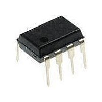
TISP61060P-S Bourns Inc., TISP61060P-S Datasheet

TISP61060P-S
Specifications of TISP61060P-S
Related parts for TISP61060P-S
TISP61060P-S Summary of contents
Page 1
... Terminal typical application names shown in P Package (Top View) Functional Replacement Terminal typical application names shown in With Lead Free Termination Finish TISP61060P-S Device Symbol TISP61060D-S TISP61060DR-S Terminals K1, K2 and A correspond to the alternative line designators and and C. The negative protection voltage is controlled by the ...
Page 2
TISP61060 Gated Protector Series Absolute Maximum Ratings Repetitive peak off-state voltage -40 °C ≤ Repetitive peak gate-cathode voltage Non-repetitive peak on-state pulse current (see Notes 1 and 2) 10/1000 µs 10/160 µs 2/10 ...
Page 3
TISP61060 Gated Protector Series ° ≤ Electrical Characteristics, - Parameter Forward voltage Holding current ...
Page 4
TISP61060 Gated Protector Series Parameter Measurement Information V GK(BO (BO (BO) Quadrant III Switching Characteristic + FSP TSP FSM TSM ...
Page 5
TISP61060 Gated Protector Series General Thyristor based overvoltage protectors, for telecommunications equipment, became popular in the late 1970s. These were fixed voltage breakover triggered devices, likened to solid state gas discharge tubes. As these were new forms of thyristors, the ...
Page 6
TISP61060 Gated Protector Series Cross-Reference for TISP61060 and LB1201AB TISP 61060 Parameter Ratings & Characteristics Non-repetitive peak on-state pulse curr ent Non-repetitive peak on-state cu rrent On-state voltage Switching current Breakover voltage Maximum continuous on- state curr ent Maximum continuous ...
Page 7
TISP61060 Gated Protector Series Electrical Characteristics The electrical characteristics of a thyristor overvoltage protector are strongly dependent on junction temperature, T value will depend on the junction temperature at the instant of measurement. The values given in this data sheet ...
Page 8
TISP61060 Gated Protector Series Impulse Protection Performance The impulse protection voltage will be the sum of the gate supply (V provides the pulse of gate current that occurs during fast rising impulses. The protection voltage will be increased if there ...
Page 9
TISP61060 Gated Protector Series AC Protection Performance (continued) However, often the supply is generated from a switching mode power supply or the SLIC supply feed has a series diode which blocks reverse (charging) current flow to the battery. In these ...
Page 10
TISP61060 Gated Protector Series TISP61060 Buffered Gate Protector (Continued) TIP WIRE 600 Ω GENERATOR SOURCE RESISTANCE 600 Ω RING WIRE A.C. GENERATOR 0 - 600 Vrms 10 0 -10 -20 -30 V -40 G -50 -60 0 300 200 100 ...
Page 11
TISP61060 Gated Protector Series TISP61060 Buffered Gate Protector (Continued) 25 Figure 4. Condition Figure 6. Condition -10 0 Figure 7. Average Gate Current vs AC Supply Voltage in Figures 2 And 5 Circuit Component ...
Page 12
TISP61060 Gated Protector Series Circuit Component Values (Continued) This table shows that the TISP61060 has impulse ratings which are higher or equal to those of the other three devices. Similarly, the TISP61060 has a.c. ratings which are higher or equal ...
Page 13
TISP61060 Gated Protector Series D008 Plastic Small-outline Package This small-outline package consists of a circuit mounted on a lead frame and encapsulated within a plastic compound. The compound will withstand soldering temperature with no deformation, and circuit performance characteristics will ...
Page 14
TISP61060 Gated Protector Series D008 Tape DImensions D008 Package (8-pin Small Outline) Single-Sprocket Tape 7.90 - 8.10 (.311 - .319) 6.30 - 6.50 (.248 - .256) Carrier Tape Embossment MILLIMETERS DIMENSIONS ARE: (INCHES) NOTES: A. Taped devices are supplied on ...
Page 15
TISP61060 Gated Protector Series P008 - Plastic Dual-In-Line Package This dual-in-line package consists of a circuit mounted on a lead frame and encapsulated within a plastic compound. The compound will withstand soldering temperature with no deformation, and circuit performance characteristics ...


