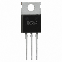
BYQ28E-200,127 NXP Semiconductors, BYQ28E-200,127 Datasheet - Page 2

BYQ28E-200,127
Manufacturer Part Number
BYQ28E-200,127
Description
DIODE RECT UFAST 200V TO220AB
Manufacturer
NXP Semiconductors
Datasheet
1.BYQ28E-200127.pdf
(4 pages)
Specifications of BYQ28E-200,127
Package / Case
TO-220AB-3
Voltage - Forward (vf) (max) @ If
1.25V @ 10A
Current - Reverse Leakage @ Vr
10µA @ 200V
Current - Average Rectified (io) (per Diode)
10A
Voltage - Dc Reverse (vr) (max)
200V
Reverse Recovery Time (trr)
25ns
Diode Type
Standard
Speed
Fast Recovery =< 500ns, > 200mA (Io)
Diode Configuration
1 Pair Common Cathode
Mounting Type
Through Hole
Product
Ultra Fast Recovery Rectifier
Configuration
Dual Common Cathode
Reverse Voltage
200 V
Forward Voltage Drop
1.25 V
Recovery Time
25 ns
Forward Continuous Current
10 A
Max Surge Current
55 A
Reverse Current Ir
10 uA
Mounting Style
Through Hole
Maximum Operating Temperature
+ 150 C
Minimum Operating Temperature
- 40 C
Lead Free Status / RoHS Status
Lead free / RoHS Compliant
Lead Free Status / RoHS Status
Lead free / RoHS Compliant, Lead free / RoHS Compliant
Other names
568-3430-5
934014550127
BYQ28E-200
934014550127
BYQ28E-200
Dissipation in the boost converter PFC circuit
Figure 1 represents a simplified structure of the primary stage
of an AC-to-DC boost converter PFC circuit of an SMPS
application. Power dissipation is the most important criterion
for circuit design. In the boost converter, power dissipation is
composed of:
1. On-state losses at the PFC diode
2. Switch-off losses at the PFC diode
3. On-state losses at the MOSFET
4. Switch-on losses at the PFC diode
5. Switching (gate-charge) losses of the MOSFET
period
t
t
t
t
t
0
1
2
3
0
time
to t
to t
to t
to t
to t
V
0
o
t
1
2
3
4
4
0
discharge gate
switching off
switching on
capacitance
charge and
operation
conducts
MOSFET
conducts
diode
diode
diode
Fig 1. Elementary boost converter PFC circuit
Fig 2. Time-voltage diagram of node A (V
Table 1. Energy loss in distinct time periods
t
1
V
t
i
2
conducting
P
----- - V
V
--------------- R
V
1
-- -
2
MOSFET
V
P
T
∫
0
o
o
i
i
⋅
⋅
(
V
o
T
⋅
⋅
V
------------------ -
V
V
FR
2
Q
o
G
o
2
F
V
r
overshoot
⋅
⋅
⋅
+
i
⋅
I
P
⎛
⎝
G
1
-- -
2
DSon
1
o
) t d
⋅
⋅
–
V
V
------------------ -
-------------- -
I
----- -
V
C
A
V
G off
o
total energy loss
2
⋅
o
(
t
i
V
GD
3
⎞ T
⎠
T
⋅
i
⋅
P
)
o
+
⋅
t
1
-- -
2
4
------------- -
I
C
G on
conducting
(= new t
⋅
GD
(
(
brb331
diode
V
FR
)
V
o
0
–
)
V
A
F
)
)
⋅
P
----- - t
V
brb332
o
o
⋅
fr
Better key characteristics at higher temperatures
Enables the use of:
- Smaller heat sink to reduce cost and space
- Low-rated MOSFET to reduce costs.
As the temperature rises, the V
drop faster than that of any other competitiors. Figure 3 shows
BYC8X-600 has the lowest V
circuit, lower V
improving the efficiency of the system
The t
temperature rises. Figure 4 shows BYC8X-600 has the shortest
t
lower temperature of the MOSFET, thus improving the
efficiency of the system.
Fig 4. The t
rr
above 104 °C. In the application circuit, shorter t
(V)
(ns)
V
t
F
rr
Fig 3. The V
rr
2.8
2.6
2.4
2.2
2.0
1.8
1.6
50
45
40
35
30
25
20
of NXP PFC diodes tends to increase more slowly as the
20
20
rr
of NXP PFC diodes tends to increase at a slower rate
Reverse recovery time as a function of temperature
BYC8X-600
competitor 1
competitor 2
competitor 3
BYC8X-600
competitor 1
competitor 2
competitor 3
F
F
will lead to a lower body temperature, thus
Forward voltage as a function of temperature
of NXP PFC diodes tends to drop faster as
40
40
as temperature rises
temperature rises
60
60
F
above 84 °C. In the application
F
of NXP PFC diodes tends to
80
80
84 °C
Date of release: May 2009
100
100
104 °C
T (°C)
T (°C)
rr
will lead to
120
120
brb336
brb335


