BAV99LT1 ON Semiconductor, BAV99LT1 Datasheet
BAV99LT1
Specifications of BAV99LT1
Available stocks


Related parts for BAV99LT1


BAV99LT1 Summary of contents
Page 1
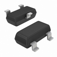
... MARKING DIAGRAM Device Code M = Date Code Pb−Free Package (Note: Microdot may be in either location) vary depending upon manufacturing location. ORDERING INFORMATION Device Package Shipping SOT−23 3000/Tape & Reel (Pb−Free) SOT−23 10,000/Tape & Reel (Pb−Free) Publication Order Number: BAV99LT1/D † ...
Page 2
OFF CHARACTERISTICS (T = 25°C unless otherwise noted) (Each Diode) A Characteristic Reverse Breakdown Voltage 100 mA) (BR) Reverse Voltage Leakage Current Vdc Vdc Vdc, T ...
Page 3
... E STYLE 11: PIN 1. ANODE 2. CATHODE 3. CATHODE-ANODE 2.0 0.079 mm inches ON Semiconductor Website: www.onsemi.com Order Literature: http://www.onsemi.com/orderlit For additional information, please contact your local Sales Representative BAV99LT1/D MAX 0.044 0.004 0.020 0.007 0.120 0.055 0.081 0.012 0.029 0.104 ...