MURD620CTT4G ON Semiconductor, MURD620CTT4G Datasheet - Page 2
MURD620CTT4G
Manufacturer Part Number
MURD620CTT4G
Description
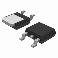
DIODE ULTRA FAST 200V 3A DPAK
Manufacturer
ON Semiconductor
Series
SWITCHMODE™r
Datasheet
1.MURD620CTG.pdf
(4 pages)
Specifications of MURD620CTT4G
Voltage - Forward (vf) (max) @ If
1V @ 3A
Current - Reverse Leakage @ Vr
5µA @ 200V
Current - Average Rectified (io) (per Diode)
3A
Voltage - Dc Reverse (vr) (max)
200V
Reverse Recovery Time (trr)
35ns
Diode Type
Standard
Speed
Fast Recovery =< 500ns, > 200mA (Io)
Diode Configuration
1 Pair Common Cathode
Mounting Type
Surface Mount
Package / Case
DPak, TO-252 (2 leads+tab), SC-63
Product
Ultra Fast Recovery Rectifier
Configuration
Dual Common Cathode
Reverse Voltage
200 V
Forward Voltage Drop
1.2 V
Recovery Time
35 ns
Forward Continuous Current
6 A
Max Surge Current
50 A
Reverse Current Ir
5 uA
Mounting Style
SMD/SMT
Maximum Operating Temperature
+ 175 C
Minimum Operating Temperature
- 65 C
Rectifier Type
Switching Diode
Peak Rep Rev Volt
200V
Avg. Forward Curr (max)
6A
Rev Curr
5uA
Peak Non-repetitive Surge Current (max)
50A
Forward Voltage
1.2V
Operating Temp Range
-65C to 175C
Package Type
DPAK
Rev Recov Time
35ns
Operating Temperature Classification
Military
Mounting
Surface Mount
Pin Count
2 +Tab
Lead Free Status / RoHS Status
Lead free / RoHS Compliant
Other names
MURD620CTT4GOS
MURD620CTT4GOS
MURD620CTT4GOSTR
MURD620CTT4GOS
MURD620CTT4GOSTR
Available stocks
Company
Part Number
Manufacturer
Quantity
Price

Part Number:
MURD620CTT4G
Manufacturer:
ON/安森美
Quantity:
20 000


2. Pulse Test: Pulse Width = 300 ms, Duty Cycle ≤ 2.0%.
ELECTRICAL CHARACTERISTICS
Maximum Instantaneous Forward Voltage Drop (Note 2)
Maximum Instantaneous Reverse Current (Note 2)
Maximum Reverse Recovery Time
100
7.0
5.0
3.0
2.0
1.0
0.7
0.5
0.3
0.2
0.1
(i
(i
(i
(i
(T
(T
(I
(I
70
50
30
20
10
F
F
F
F
F
F
J
J
= 3 Amps, T
= 3 Amps, T
= 6 Amps, T
= 6 Amps, T
= 1 Amp, di/dt = 50 Amps/ms, V
= 0.5 Amp, i
= 25°C, Rated dc Voltage)
= 125°C, Rated dc Voltage)
0
Figure 1. Typical Forward Voltage (Per Leg)
0.2
v
C
C
C
C
R
F,
= 25°C)
= 125°C)
= 25°C)
= 125°C)
= 1 Amp, I
INSTANTANEOUS VOLTAGE (V)
0.4
150°C
175°C
REC
0.6
= 0.25 A, V
R
0.8
= 30 V, T
(Per Diode)
Rating
R
100°C
T
1.0
J
= 30 V, T
J
= 25°C
= 25°C)
1.2
J
http://onsemi.com
= 25°C)
1.4
2
0.0001
0.001
0.01
9.0
8.0
7.0
6.0
5.0
4.0
3.0
2.0
1.0
100
0.1
14
13
12
10
11
10
0
1
0
0
* The curves shown are typical for the highest voltage device in the
voltage grouping. Typical reverse current for lower voltage selections
can be estimated from these curves if V
V
Figure 3. Average Power Dissipation (Per Leg)
R
Figure 2. Typical Leakage Current* (Per Leg)
.
1.0
20
I
PK
I
F(AV)
/I
AV
2.0
40
= 20
, AVERAGE FORWARD CURRENT (A)
150°C
V
3.0
R
60
, REVERSE VOLTAGE (V)
Symbol
v
i
t
4.0
R
rr
F
10
80
T
100°C
J
25°C
100 120 140 160 180 200
5.0
= 175°C
R
6.0
5.0
is sufficiently below rated
Value
0.96
1.13
250
1.2
35
25
1
5
WAVE
SINE
7.0
T
8.0
J
= 175°C
SQUARE
WAVE
9.0
Unit
mA
ns
V
dc
10
Related parts for MURD620CTT4G
Image
Part Number
Description
Manufacturer
Datasheet
Request
R

Part Number:
Description:
ON Semiconductor [VOLTAGE REGULATOR]
Manufacturer:
ON Semiconductor
Datasheet:
Part Number:
Description:
357-036-542-201 CARDEDGE 36POS DL .156 BLK LOPRO
Manufacturer:
ON Semiconductor
Datasheet:
Part Number:
Description:
357-036-542-201 CARDEDGE 36POS DL .156 BLK LOPRO
Manufacturer:
ON Semiconductor
Datasheet:
Part Number:
Description:
357-036-542-201 CARDEDGE 36POS DL .156 BLK LOPRO
Manufacturer:
ON Semiconductor
Datasheet:
Part Number:
Description:
357-036-542-201 CARDEDGE 36POS DL .156 BLK LOPRO
Manufacturer:
ON Semiconductor
Datasheet:
Part Number:
Description:
357-036-542-201 CARDEDGE 36POS DL .156 BLK LOPRO
Manufacturer:
ON Semiconductor
Datasheet:
Part Number:
Description:
357-036-542-201 CARDEDGE 36POS DL .156 BLK LOPRO
Manufacturer:
ON Semiconductor
Datasheet:
Part Number:
Description:
357-036-542-201 CARDEDGE 36POS DL .156 BLK LOPRO
Manufacturer:
ON Semiconductor
Datasheet:
Part Number:
Description:
357-036-542-201 CARDEDGE 36POS DL .156 BLK LOPRO
Manufacturer:
ON Semiconductor
Datasheet:
Part Number:
Description:
357-036-542-201 CARDEDGE 36POS DL .156 BLK LOPRO
Manufacturer:
ON Semiconductor
Datasheet:
Part Number:
Description:
357-036-542-201 CARDEDGE 36POS DL .156 BLK LOPRO
Manufacturer:
ON Semiconductor
Datasheet:
Part Number:
Description:
Manufacturer:
ON Semiconductor
Datasheet:
Part Number:
Description:
Manufacturer:
ON Semiconductor
Datasheet:
Part Number:
Description:
Manufacturer:
ON Semiconductor
Datasheet: