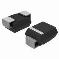
MBRS2040LT3G ON Semiconductor, MBRS2040LT3G Datasheet - Page 4

MBRS2040LT3G
Manufacturer Part Number
MBRS2040LT3G
Description
DIODE SCHOTTKY 40V 2A SMB
Manufacturer
ON Semiconductor
Specifications of MBRS2040LT3G
Voltage - Forward (vf) (max) @ If
430mV @ 2A
Voltage - Dc Reverse (vr) (max)
40V
Current - Average Rectified (io)
2A
Current - Reverse Leakage @ Vr
800µA @ 40V
Diode Type
Schottky
Speed
Fast Recovery =< 500ns, > 200mA (Io)
Mounting Type
Surface Mount
Package / Case
DO-214AA, SMB
Product
Schottky Diodes
Peak Reverse Voltage
40 V
Forward Continuous Current
2 A
Max Surge Current
70 A
Configuration
Single
Forward Voltage Drop
0.5 V @ 4 A
Maximum Reverse Leakage Current
800 uA
Operating Temperature Range
- 55 C to + 125 C
Mounting Style
SMD/SMT
Current, Forward
2 A
Current, Reverse
20 mA
Current, Surge
70 A
Package Type
SMB
Primary Type
Schottky Barrier
Temperature, Junction, Maximum
+125 °C
Temperature, Operating
-55 to +125 °C
Voltage, Forward
0.43 V
Voltage, Reverse
40 V
Rectifier Type
Schottky Diode
Peak Rep Rev Volt
40V
Avg. Forward Curr (max)
2A
Rev Curr
800uA
Peak Non-repetitive Surge Current (max)
70A
Forward Voltage
0.5V
Operating Temp Range
-55C to 125C
Operating Temperature Classification
Military
Mounting
Surface Mount
Pin Count
2
Lead Free Status / RoHS Status
Lead free / RoHS Compliant
Reverse Recovery Time (trr)
-
Capacitance @ Vr, F
-
Lead Free Status / Rohs Status
Lead free / RoHS Compliant
Other names
MBRS2040LT3GOSTR
Available stocks
Company
Part Number
Manufacturer
Quantity
Price
Part Number:
MBRS2040LT3G
Manufacturer:
ON/安森美
Quantity:
20 000
1000
100
0.001
0.001
10
0.01
0.01
1.0
0.1
1.0
0.1
0
0.00001
0.00001
5.0%
2.0%
1.0%
50%
20%
10%
5.0%
2.0%
1.0%
50%
20%
10%
* Reverse power dissipation and the possibility of thermal runaway must be considered when operating this device under any re-
verse voltage conditions. Calculations of T J therefore must include forward and reverse power effects. The allowable operating
T J may be calculated from the equation:
This graph displays the derated allowable T J due to reverse bias under DC conditions only and is calculated as T J = T Jmax − r(t)Pr,
where r(t) = Rthja. For other power applications further calculations must be performed.
5.0
10
V R , REVERSE VOLTAGE (VOLTS)
0.0001
Figure 7. Capacitance
0.0001
15
Rtjl(t) = Rtjl*r(t)
20
Figure 10. Thermal Response Junction to Ambient
0.001
Figure 9. Thermal Response Junction to Lead
25
0.001
T J = 25 C
Rtjl(t) = Rtjl*r(t)
30
0.01
35
r(t) = thermal impedance under given conditions,
Pf = forward power dissipation, and
Pr = reverse power dissipation
T J = T Jmax − r(t)(Pf + Pr) where
http://onsemi.com
MBRS2040LT3
0.01
T, TIME (s)
T, TIME (s)
40
4
0.1
125
105
115
95
85
75
65
Figure 8. Typical Operating Temperature Derating*
0
0.1
5.0
1.0
V R , DC REVERSE VOLTAGE (VOLTS)
10
1.0
15
10
20
42 C/W
61 C/W
25
10
78 C/W
100
30
R tja = 22.5 C/W
92 C/W
35
1,000
100
40


