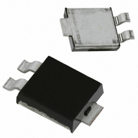
Mechanical Data
Notes:
Features
·
·
·
·
·
·
·
·
Maximum Ratings
Single phase, half wave, 60Hz, resistive or inductive load.
For capacitive load, derate current by 20%.
DS30255 Rev. 11 - 3
·
·
·
·
·
·
·
·
Electrical Characteristics
Peak Repetitive Reverse Voltage
Working Peak Reverse Voltage
DC Blocking Voltage
RMS Reverse Voltage
Average Rectified Output Current (see also Figure 4)
Non-Repetitive Peak Forward Surge Current
8.3ms Single half sine-wave Superimposed on Rated Load
Typical Thermal Resistance Junction to Soldering Point
Operating Temperature Range
Storage Temperature Range
Reverse Breakdown Voltage (Note 1)
Forward Voltage
Reverse Current (Note 1)
Total Capacitance
Guard Ring Die Construction for Transient Protection
Low Power Loss, High Efficiency
High Surge Capability
High Max Junction Temperature Rating
Low Forward Voltage Drop
Very Low Leakage Current
For Use in Low Voltage, High Frequency Inverters, Free
Wheeling, and Polarity Protection Applications
Available in Lead Free Finish/RoHS Compliant Version
(Note 2)
Case: POWERMITEâ3
Case Material: Molded Plastic. UL Flammability
Classification Rating 94V-0
Moisture Sensitivity: Level 1 per J-STD-020C
Terminals: Solderable per MIL-STD-202, Method 208
Also available in Lead Free Plating (Matte Tin Finish).
Please see Ordering Information, Note 12, on Page 3
Polarity: See Diagram
Marking Information: See Page 3
Weight: 0.072 grams (approximate)
1. Short duration test pulse used to minimize self-heating effect.
2. RoHS revision 13.2.2003. Glass and High Temperature Solder Exemptions Applied, see EU Directive Annex Notes 5 and 7.
Characteristic
Characteristic
@ T
A
= 25°C unless otherwise specified
@ T
@ T
A
= 25°C unless otherwise specified
C
= 88°C
www.diodes.com
Note:
Symbol
V
C
10A LOW VF SCHOTTKY BARRIER RECTIFIER
(BR)R
1 of 3
C
V
I
R
F
T
PIN 2
1
PIN 1
Symbol
V
P
Pins 1 & 2 must be electrically
connected at the printed circuit board.
V
A
V
3
D
T
R(RMS)
R
I
FSM
RWM
V
RRM
I
STG
T
qJS
O
R
j
Min
2
40
¾
¾
¾
¾
¾
¾
C
B
0.45
0.47
12.5
Typ
700
0.1
¾
¾
M
E
L
PIN 3, BOTTOMSIDE
HEAT SINK
Max
0.49
0.41
0.51
0.3
25
¾
¾
K
J
-65 to +150
-65 to +150
G
H
Value
Unit
mA
pF
150
2.5
V
V
40
28
10
SBM1040
I
I
I
I
T
T
f = 1.0MHz, V
POWERMITEâ3
R
F
F
F
S
S
= 8A, T
= 8A, T
= 10A, T
= 1mA
= 25°C, V
= 100°C, V
All Dimensions in mm
Dim
A
B
C
D
G
H
K
M
E
J
L
P
Test Condition
POWERMITEâ3
ã
S
S
S
= 25°C
= 125°C
Diodes Incorporated
= 25°C
4.03
6.40
.864
1.10
.173
5.01
4.37
.173
1.73
Min
R
.71
.36
R
R
1.83 NOM
= 4.0V DC
= 35V
= 35V
SBM1040
°C/W
Unit
°C
°C
V
V
A
A
Max
4.09
6.61
.914
1.14
.203
5.17
4.43
.203
1.83
.77
.46