MBRA340T3G ON Semiconductor, MBRA340T3G Datasheet
MBRA340T3G
Specifications of MBRA340T3G
Available stocks


Related parts for MBRA340T3G

MBRA340T3G Summary of contents
Page 1
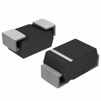
... Pb−Free Package ORDERING INFORMATION Device Package Shipping MBRA340T3 SMA 5000/Tape & Reel SMA MBRA340T3G 5000/Tape & Reel (Pb−Free) †For information on tape and reel specifications, including part orientation and tape sizes, please refer to our Tape and Reel Packaging Specification Brochure, BRD8011/D. 2 † ...
Page 2
THERMAL CHARACTERISTICS Characteristic Thermal Resistance − Junction−to−Lead (Note 2) Thermal Resistance − Junction−to−Ambient (Note 2) ELECTRICAL CHARACTERISTICS Maximum Instantaneous Forward Voltage (Note 3) Maximum Instantaneous Reverse Current 2. Mounted on 2″ Square PC Board with 1″ Square Total Pad Size, ...
Page 3
... D POLARITY INDICATOR OPTIONAL AS NEEDED (SEE STYLES *For additional information on our Pb−Free strategy and soldering details, please download the ON Semiconductor Soldering and Mounting Techniques Reference Manual, SOLDERRM/D. MBRA340T3 PACKAGE DIMENSIONS SMA CASE 403D−02 ISSUE C NOTES: 1. DIMENSIONING AND TOLERANCING PER ANSI Y14 ...