STGP19NC60WD STMicroelectronics, STGP19NC60WD Datasheet
STGP19NC60WD
Specifications of STGP19NC60WD
Available stocks


Related parts for STGP19NC60WD


STGP19NC60WD Summary of contents
Page 1
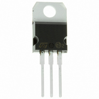
... STGP19NC60WD STGW19NC60WD May 2007 N-channel 600V - 19A - TO-220 - TO-247 Ultra fast PowerMESH™ IGBT V I CE(sat) C @100°C < 2.5V 22A < 2.5V 23A Internal schematic diagram Marking GP19NC60WD GW19NC60WD Rev 3 STGW19NC60WD STGP19NC60WD TO-220 TO-247 Package Packaging TO-220 Tube TO-247 Tube 1/15 www.st.com 15 ...
Page 2
... Contents Contents 1 Electrical ratings . . . . . . . . . . . . . . . . . . . . . . . . . . . . . . . . . . . . . . . . . . . . 3 2 Electrical characteristics . . . . . . . . . . . . . . . . . . . . . . . . . . . . . . . . . . . . . 4 2.1 Electrical characteristics (curves) 3 Test circuit 4 Package mechanical data . . . . . . . . . . . . . . . . . . . . . . . . . . . . . . . . . . . . 11 5 Revision history . . . . . . . . . . . . . . . . . . . . . . . . . . . . . . . . . . . . . . . . . . . 14 2/ STGP19NC60WD - STGW19NC60WD . . . . . . . . . . . . . . . . . . . . . . . . . . . . 7 ...
Page 3
... STGP19NC60WD - STGW19NC60WD 1 Electrical ratings Table 1. Absolute maximum ratings Symbol V Collector-emitter voltage (V CES (1) Collector current (continuous (1) Collector current (continuous (2) Collector current (pulsed Diode RMS forward current Gate-emitter voltage GE P Total dissipation at T TOT T Storage temperature stg T Operating junction temperature j 1. Calculated according to the iterative formula: 2. Vclamp=480V, Tj=150° ...
Page 4
... Max rating Max rating ±20V 15V Parameter Test conditions V = 25V 1MHz 390V 15V, GE Figure 16 STGP19NC60WD - STGW19NC60WD Min. Typ 600 = 12A 2.1 =12A,Tc=125°C 1.8 = 250 µA 3.75 = 25° 125° 12A 10 Min. Typ. 1180 130 Max. Unit V 2 5.75 V 150 µ ...
Page 5
... STGP19NC60WD - STGW19NC60WD Table 5. Switching on/off (inductive load) Symbol t Turn-on delay time d(on) t Current rise time r Turn-on current slope (di/dt Turn-on delay time d(on) t Current rise time r Turn-on current slope (di/dt Off voltage rise time r off Turn-off delay time d off Current fall time ...
Page 6
... Reverse recovery time rr Q Reverse recovery charge rr Reverse recovery current I rrm 6/15 Parameter Test conditions I = 12A 12A 125° 12A,V = 50V 25°C, di/dt = 100 A/µs Figure 12A,V = 50V =125°C, di/dt = 100A/µs Figure 18 STGP19NC60WD - STGW19NC60WD Min. Typ. Max. 1.9 2.5 1 102 4 Unit ...
Page 7
... STGP19NC60WD - STGW19NC60WD 2.1 Electrical characteristics (curves) Figure 1. Output characteristics Figure 3. Transconductance Figure 5. Gate charge vs gate-source voltage Figure 6. Electrical characteristics Figure 2. Transfer characteristics Figure 4. Collector-emitter on voltage vs temperature Capacitance variations 7/15 ...
Page 8
... Electrical characteristics Figure 7. Normalized gate threshold voltage vs temperature Figure 9. Normalized breakdown voltage vs temperature Figure 11. Switching losses vs gate resistance Figure 12. Switching losses vs collector 8/15 STGP19NC60WD - STGW19NC60WD Figure 8. Collector-emitter on voltage vs collector current Figure 10. Switching losses vs temperature current ...
Page 9
... STGP19NC60WD - STGW19NC60WD Figure 13. Turn-off SOA Electrical characteristics Figure 14. Emitter-collector diode characteristics 9/15 ...
Page 10
... Test circuit 3 Test circuit Figure 15. Test circuit for inductive load switching Figure 17. Switching waveform 10/15 STGP19NC60WD - STGW19NC60WD Figure 16. Gate charge test circuit Figure 18. Diode recovery time waveform ...
Page 11
... STGP19NC60WD - STGW19NC60WD 4 Package mechanical data In order to meet environmental requirements, ST offers these devices in ECOPACK® packages. These packages have a Lead-free second level interconnect. The category of second level interconnect is marked on the package and on the inner box label, in compliance with JEDEC Standard JESD97. The maximum ratings related to soldering conditions are also marked on the inner box label ...
Page 12
... Package mechanical data Dim L20 L30 ∅P Q 12/15 STGP19NC60WD - STGW19NC60WD TO-220 mechanical data mm Min Typ Max 4.40 4.60 0.61 0.88 1.14 1.70 0.49 0.70 15.25 15.75 1.27 10 10.40 2.40 2.70 4.95 5.15 1.23 1.32 6.20 6.60 2.40 2. 3.50 3.93 16.40 28.90 3 ...
Page 13
... STGP19NC60WD - STGW19NC60WD DIM øP øR S TO-247 MECHANICAL DATA mm. MIN. TYP MAX. 4.85 5.15 2.20 2.60 1.0 1.40 2.0 2.40 3.0 3.40 0.40 0.80 19.85 20.15 15.45 15.75 5.45 14.20 14.80 3.70 4.30 18.50 3.55 3.65 4.50 5.50 5.50 Package mechanical data inch MIN ...
Page 14
... Revision history 5 Revision history Table 8. Revision history Date 04-Oct-2006 13-Apr-2007 08-May-2007 14/15 Revision 1 Initial release. 2 Final version 3 Added TO-247 STGP19NC60WD - STGW19NC60WD Changes ...
Page 15
... STGP19NC60WD - STGW19NC60WD Information in this document is provided solely in connection with ST products. STMicroelectronics NV and its subsidiaries (“ST”) reserve the right to make changes, corrections, modifications or improvements, to this document, and the products and services described herein at any time, without notice. All ST products are sold pursuant to ST’s terms and conditions of sale. ...