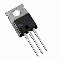
IRG4BC10SDPBF International Rectifier, IRG4BC10SDPBF Datasheet

IRG4BC10SDPBF
Specifications of IRG4BC10SDPBF
Available stocks
Related parts for IRG4BC10SDPBF
IRG4BC10SDPBF Summary of contents
Page 1
... R Junction-to-Case - Diode θJC R Case-to-Sink, flat, greased surface θCS R Junction-to-Ambient, typical socket mount θJA Wt Weight www.irf.com IRG4BC10SDPbF G TM ultrafast, n-channel 300 (0.063 in. (1.6mm) from case) Min. ––– ––– ––– ––– ––– ...
Page 2
... IRG4BC10SDPbF Electrical Characteristics @ T Parameter V Collector-to-Emitter Breakdown Voltage (BR)CES ∆V Temperature Coeff. of Breakdown Voltage /∆T (BR)CES J V Collector-to-Emitter Saturation Voltage CE(on) V Gate Threshold Voltage GE(th) ∆V /∆T Temperature Coeff. of Threshold Voltage GE(th Forward Transconductance fe I Zero Gate Voltage Collector Current CES V Diode Forward Voltage Drop ...
Page 3
... Fig Typical Load Current vs. Frequency 100 ° 80µs PULSE WIDTH 1 0.5 1.0 1.5 2 Collector-to-Emitter Voltage (V) CE Fig Typical Output Characteristics www.irf.com IRG4BC10SDPBF Frequency (KHz) (Load Current = I of fundamental) RMS 100 ° 150 150 15V 1 2.5 3.0 6 Fig Typical Transfer Characteristics ...
Page 4
... IRG4BC10SDPbF 100 T , Case Temperature ( C) C Fig Maximum Collector Current vs. Case Temperature 0.50 1 0.20 0.10 0.05 0.02 SINGLE PULSE 0.01 0.1 (THERMAL RESPONSE) 0.01 0.00001 0.0001 Fig Maximum Effective Transient Thermal Impedance, Junction-to-Case 4 3. 15V PULSE WIDTH 2.50 2.00 1.50 1.00 -60 -40 -20 ...
Page 5
... Fig Typical Capacitance vs. Collector-to-Emitter Voltage 3. 480V 15V GE ° 3. 3.50 3.45 3.40 3.35 3. Gate Resistance (Ohm Gate Resistance (Ω) G Fig Typical Switching Losses vs. Gate Resistance www.irf.com IRG4BC10SDPBF SHORTED 100 0 Fig Typical Gate Charge vs. 100 0.1 80 100 -60 -40 -20 Fig Typical Switching Losses vs. = 400V = ...
Page 6
... IRG4BC10SDPbF 15 Ω 100 150 C ° 480V 15V Collector Current (A) C Fig Typical Switching Losses vs. Collector Current 100 10 1 0.1 0.0 6 100 SAFE OPERATING AREA 150° 125° 25°C J 1.0 2.0 3.0 4.0 5.0 6.0 Forward Voltage Drop - V ( 20V = 125 100 ...
Page 7
... J 20 100 di /dt - (A/µs) f Fig Typical Reverse Recovery vs. di 200 V = 200V 125° 25°C J 160 4.0A F 120 100 di /dt - (A/µs) f Fig Typical Stored Charge vs. di www.irf.com IRG4BC10SDPBF 200V 125° 25° 1000 100 Fig Typical Recovery Current vs. di /dt ...
Page 8
... IRG4BC10SDPbF 430µF 80% of Vce Fig. 18a - Test Circuit for Measurement off(diode d(on) GATE VOLTAGE D.U.T. 10% +Vg +Vg Vce 10% Ic Vcc 90 Vce tr td(on) t1 Fig. 18c - Test Waveforms for Circuit of Fig. 18a, Defining d(on) 8 Same type device as D.U.T. D.U. 90% 10 d(off d(on) Fig. 18b - Test Waveforms for Circuit of Fig ...
Page 9
... Figure 18e. Macro Waveforms for L 1000V 50V 6000µF 100V Figure 19. Clamped Inductive Load Test Circuit www.irf.com IRG4BC10SDPBF Vg GATE SIGNAL DEVICE UNDER TEST CURRENT D.U.T. VOLTAGE IN D.U.T. CURRENT Figure 18a's D.U. Figure 20. Pulsed Collector Current Test Circuit L C Test Circuit 9 ...
Page 10
... IRG4BC10SDPbF Notes: Repetitive rating: V =20V; pulse width limited by maximum junction temperature (figure 20) GE ‚V =80%( =20V, L=10µ CES GE ƒPulse width ≤ duty factor ≤ „Pulse width single shot. IR WORLD HEADQUARTERS: 233 Kansas St., El Segundo, California 90245, USA Tel: (310) 252-7105 10 = 100W (figure 19) G ...


