NGB18N40CLBT4 ON Semiconductor, NGB18N40CLBT4 Datasheet

IGBT N-CHAN 18A 400V ESD D2PAK

NGB18N40CLBT4

Manufacturer Part Number
NGB18N40CLBT4
Description
IGBT N-CHAN 18A 400V ESD D2PAK
Manufacturer
ON Semiconductor
Datasheet

Specifications of NGB18N40CLBT4

Voltage - Collector Emitter Breakdown (max)
430V
Vce(on) (max) @ Vge, Ic
2V @ 4.5V, 10A
Current - Collector (ic) (max)
18A
Power - Max
115W
Input Type
Logic
Mounting Type
Surface Mount
Package / Case
D²Pak, TO-263 (2 leads + tab)
Product
Electronic Ignition Drivers
Mounting Style
SMD/SMT
Lead Free Status / RoHS Status
Contains lead / RoHS non-compliant
Igbt Type
-
Lead Free Status / Rohs Status
Lead free / RoHS Compliant
Other names
NGB18N40CLBT4OS

Available stocks

Company
Part Number
Manufacturer
Quantity
Price
Part Number:
NGB18N40CLBT4
0
Part Number:
NGB18N40CLBT4G
Manufacturer:
ON Semiconductor
Quantity:
500
Part Number:
NGB18N40CLBT4G
Manufacturer:
ON
Quantity:
12 500
NGB18N40CLBT4
Ignition IGBT
18 Amps, 400 Volts
N−Channel D
monolithic circuitry integrating ESD and Over−Voltage clamped
protection for use in inductive coil drivers applications. Primary uses
include Ignition, Direct Fuel Injection, or wherever high voltage and
high current switching is required.
Features
Stresses exceeding Maximum Ratings may damage the device. Maximum
Ratings are stress ratings only. Functional operation above the Recommended
Operating Conditions is not implied. Extended exposure to stresses above the
Recommended Operating Conditions may affect device reliability.
MAXIMUM RATINGS
© Semiconductor Components Industries, LLC, 2006
May, 2006 − Rev. 3
Collector−Emitter Voltage
Collector−Gate Voltage
Gate−Emitter Voltage
Collector Current−Continuous
@ T
ESD (Human Body Model)
R = 1500 W, C = 100 pF
ESD (Machine Model) R = 0 W, C = 200 pF
Total Power Dissipation @ T
Derate above 25°C
Operating and Storage Temperature Range
This Logic Level Insulated Gate Bipolar Transistor (IGBT) features
Stress Applied to Load
Per Area
Microprocessor Devices
Ideal for Coil−on−Plug Applications
Gate−Emitter ESD Protection
Temperature Compensated Gate−Collector Voltage Clamp Limits
Integrated ESD Diode Protection
New Design Increases Unclamped Inductive Switching (UIS) Energy
Low Threshold Voltage to Interface Power Loads to Logic or
Low Saturation Voltage
High Pulsed Current Capability
Integrated Gate−Emitter Resistor (R
Emitter Ballasting for Short−Circuit Capability
Pb−Free Package is Available
C
= 25°C − Pulsed
Rating
2
(T
PAK
J
= 25°C unless otherwise noted)
C
= 25°C
GE
Symbol
)
T
V
V
ESD
ESD
J
V
P
CER
, T
CES
I
GE
C
D
stg
−55 to +175
Value
0.77
430
430
800
115
8.0
18
18
50
1
W/°C
Unit
V
V
V
A
A
kV
°C
W
V
DC
DC
DC
DC
AC
†For information on tape and reel specifications,
NGB18N40CLBT4
NGB18N40CLBT4G
including part orientation and tape sizes, please
refer to our Tape and Reel Packaging Specifications
Brochure, BRD8011/D.
Device
G
GB18N40B = Device Code
A
Y
WW
G
18 AMPS, 400 VOLTS
I
ORDERING INFORMATION
C
V
= 10 A, V
MARKING DIAGRAM
Gate
CE(on)
http://onsemi.com
1
R
Collector
Collector
18N40BG
= Assembly Location
= Year
= Work Week
= Pb−Free Package
GE
(Pb−Free)
Package
AYWW
D
D
3 2.0 V @
2
4
Publication Order Number:
2
2
PAK
PAK
GE
GB
CASE 418B
STYLE 4
. 4.5 V
3
Emitter
D
NGB18N40CLB/D
2
800/Tape & Reel
800/Tape & Reel
C
E
PAK
Shipping

Related parts for NGB18N40CLBT4

NGB18N40CLBT4 Summary of contents

Page 1

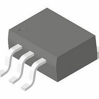
... ORDERING INFORMATION Device Package Shipping 2 NGB18N40CLBT4 D PAK 800/Tape & Reel 2 NGB18N40CLBT4G D PAK 800/Tape & Reel (Pb−Free) †For information on tape and reel specifications, including part orientation and tape sizes, please refer to our Tape and Reel Packaging Specifications Brochure, BRD8011/D. Publication Order Number: NGB18N40CLB/D † ...

Page 2

... ON CHARACTERISTICS (Note 2) Gate Threshold Voltage Threshold Temperature Coefficient (Negative) *Maximum Value of Characteristic across Temperature Range. 1. When surface mounted to an FR4 board using the minimum recommended pad size. 2. Pulse Test: Pulse Width v 300 mS, Duty Cycle v 2%. NGB18N40CLBT4 = 25° 125° 25°C J (−55°C ≤ T ≤ ...

Page 3

... Fall Time (Resistive) Turn−On Delay Time Rise Time *Maximum Value of Characteristic across Temperature Range. 1. When surface mounted to an FR4 board using the minimum recommended pad size. 2. Pulse Test: Pulse Width v 300 mS, Duty Cycle v 2%. NGB18N40CLBT4 Symbol Test Conditions Temperature V CE(on ...

Page 4

... COLLECTOR TO EMITTER VOLTAGE (VOLTS) CE Figure 3. Output Characteristics 4.0 3 3.0 2.5 2.0 1.5 1.0 0.5 0.0 −50 − JUNCTION TEMPERATURE (°C) J Figure 5. Collector−to−Emitter Saturation Voltage versus Junction Temperature NGB18N40CLBT4 (unless otherwise noted 4 −40° 3 2 COLLECTOR TO EMITTER VOLTAGE (VOLTS) CE Figure 2. Output Characteristics ...

Page 5

... TEMPERATURE (°C) Figure 9. Gate Threshold Voltage versus Temperature −50 − 100 TEMPERATURE (°C) Figure 11. Typical Open Secondary Latch Current versus Temperature NGB18N40CLBT4 10000 T = 150° 1000 iss 100 C oss 10 C rss COLLECTOR TO EMITTER VOLTAGE (VOLTS) CE Figure 8. Capacitance Variation ...

Page 6

... Figure 15. Pulse Train Safe Operating Area (Mounted on an Infinite Heatsink 0 5 Figure 17. Circuit Configuration for Short Circuit Test #1 NGB18N40CLBT4 100 DC 10 100 ms 1 0.1 0.01 100 1000 1 COLLECTOR−EMITTER VOLTAGE (VOLTS) Figure 14. Single Pulse Safe Operating Area = 255C) (Mounted on an Infinite Heatsink at T ...

Page 7

... Duty Cycle = 0.5 0.2 0.1 10 0.05 0.02 0.01 1 0.1 0.01 Single Pulse 0.001 0.0001 0.00001 0.0001 (Non−normalized Junction−to−Ambient mounted on NGB18N40CLBT4 P (pk DUTY CYCLE 0.001 0.01 t,TIME (S) Figure 19. Transient Thermal Resistance minimum pad area) http://onsemi.com 7 D CURVES APPLY FOR POWER ...

Page 8

... Literature Distribution Center for ON Semiconductor P.O. Box 5163, Denver, Colorado 80217 USA Phone: 303−675−2175 or 800−344−3860 Toll Free USA/Canada Fax: 303−675−2176 or 800−344−3867 Toll Free USA/Canada Email: orderlit@onsemi.com NGB18N40CLBT4 PACKAGE DIMENSIONS 2 D PAK 3 CASE 418B−04 ...

Related keywords