PN4091 Fairchild Semiconductor, PN4091 Datasheet

JFET SWITCH N-CHAN TO-92

PN4091

Manufacturer Part Number
PN4091
Description
JFET SWITCH N-CHAN TO-92
Manufacturer
Fairchild Semiconductor
Datasheet

Specifications of PN4091

Current - Drain (idss) @ Vds (vgs=0)
30mA @ 20V
Fet Type
N-Channel
Voltage - Breakdown (v(br)gss)
40V
Voltage - Cutoff (vgs Off) @ Id
5V @ 1nA
Input Capacitance (ciss) @ Vds
16pF @ 20V
Resistance - Rds(on)
30 Ohm
Mounting Type
Through Hole
Package / Case
TO-92-3 (Standard Body), TO-226
Power - Max
625mW
Configuration
Single
Transistor Polarity
N-Channel
Power Dissipation
625 mW
Gate-source Breakdown Voltage
- 40 V
Gate-source Cutoff Voltage
- 10 V
Drain Current (idss At Vgs=0)
0.2 mA to 0.6 mA
Resistance Drain-source Rds (on)
30 Ohms
Maximum Operating Temperature
+ 150 C
Maximum Drain Gate Voltage
40 V
Minimum Operating Temperature
- 55 C
Mounting Style
Through Hole
Lead Free Status / RoHS Status
Lead free / RoHS Compliant

Available stocks

Company
Part Number
Manufacturer
Quantity
Price
Part Number:
PN4091
Manufacturer:
SEMIKRON
Quantity:
143
Part Number:
PN4091
Manufacturer:
FSC
Quantity:
1 525
Part Number:
PN4091
Manufacturer:
FAIRCHILD
Quantity:
16 910
Part Number:
PN4091
Manufacturer:
FAIRCHILD/仙童
Quantity:
20 000
Part Number:
PN4091_D26Z
Manufacturer:
Fairchild Semiconductor
Quantity:
1 990
1997 Fairchild Semiconductor Corporation
P
R
R
V
V
I
T
Symbol
Symbol
GF
D
DG
GS
J
*
NOTES:
1) These ratings are based on a maximum junction temperature of 150 degrees C.
2) These are steady state limits. The factory should be consulted on applications involving pulsed or low duty cycle operations
*
Thermal Characteristics
N-Channel Switch
JC
JA
This device is designed for low level analog switching, sample
and hold circuits and chopper stabalized amplifiers. Sourced
from Process 51. See J111 for characteristics.
Absolute Maximum Ratings*
,T
These ratings are limiting values above which the serviceability of any semiconductor device may be impaired.
Device mounted on FR-4 PCB 1.6" X 1.6" X 0.06."
stg
Total Device Dissipation
Thermal Resistance, Junction to Case
Thermal Resistance, Junction to Ambient
Drain-Gate Voltage
Gate-Source Voltage
Forward Gate Current
Operating and Storage Junction Temperature Range
G
Derate above 25 C
S
D
PN4091
PN4092
PN4093
Characteristic
TO-92
Parameter
TA = 25°C unless otherwise noted
PN4091-4093
Mark: 61J / 61K / 61L
MMBF4091
MMBF4092
MMBF4093
625
125
357
5.0
SOT-23
G
NOTE: Source & Drain
are interchangeable
Max
-55 to +150
*MMBF4091-4093
S
Value
- 40
40
50
350
556
2.8
D
Units
mA
V
V
mW/ C
Units
C
mW
C/W
C/W

Related parts for PN4091

PN4091 Summary of contents

Page 1

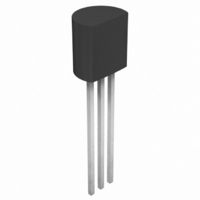
... Device mounted on FR-4 PCB 1.6" X 1.6" X 0.06." 1997 Fairchild Semiconductor Corporation MMBF4091 MMBF4092 MMBF4093 G TO-92 SOT-23 Mark: 61J / 61K / 61L TA = 25°C unless otherwise noted Parameter TA = 25°C unless otherwise noted PN4091-4093 625 5.0 125 357 D S NOTE: Source & Drain are interchangeable Value Units 40 ...

Page 2

Electrical Characteristics Symbol Parameter OFF CHARACTERISTICS V Gate-Source Breakdown Voltage (BR)GSS V Gate-Source Cutoff Voltage GS(off) I Drain-Gate Leakage Current DGO I Drain Cutoff Leakage Current D(off) ON CHARACTERISTICS I Zero-Gate Voltage Drain Current* DSS Drain-Source On Voltage V on ...

Page 3

... TRADEMARKS The following are registered and unregistered trademarks Fairchild Semiconductor owns or is authorized to use and is not intended exhaustive list of all such trademarks. ACEx™ FASTr™ Bottomless™ GlobalOptoisolator™ CoolFET™ GTO™ CROSSVOLT™ HiSeC™ DOME™ ISOPLANAR™ ...

Related keywords