FDS6990AS Fairchild Semiconductor, FDS6990AS Datasheet
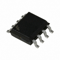
MOSFET NCH DUAL 30V 7.5A 8SOIC

FDS6990AS

Manufacturer Part Number
FDS6990AS
Description
MOSFET NCH DUAL 30V 7.5A 8SOIC
Manufacturer
Fairchild Semiconductor
Series
PowerTrench®, SyncFET™r
Datasheet

Specifications of FDS6990AS

Fet Type
2 N-Channel (Dual)
Fet Feature
Logic Level Gate
Rds On (max) @ Id, Vgs
22 mOhm @ 7.5A, 10V
Drain To Source Voltage (vdss)
30V
Current - Continuous Drain (id) @ 25° C
7.5A
Vgs(th) (max) @ Id
3V @ 1mA
Gate Charge (qg) @ Vgs
14nC @ 5V
Input Capacitance (ciss) @ Vds
550pF @ 15V
Power - Max
900mW
Mounting Type
Surface Mount
Package / Case
8-SOIC (3.9mm Width)
Configuration
Dual Dual Drain
Transistor Polarity
N-Channel
Resistance Drain-source Rds (on)
0.022 Ohm @ 10 V
Forward Transconductance Gfs (max / Min)
29 S
Drain-source Breakdown Voltage
30 V
Gate-source Breakdown Voltage
+/- 20 V
Continuous Drain Current
7.5 A
Power Dissipation
1600 mW
Maximum Operating Temperature
+ 150 C
Mounting Style
SMD/SMT
Minimum Operating Temperature
- 55 C
Dc
0512
Lead Free Status / RoHS Status
Lead free / RoHS Compliant
Other names
FDS6990AS
FDS6990ASTR

Available stocks

Company
Part Number
Manufacturer
Quantity
Price
Part Number:
FDS6990AS
Manufacturer:
INFINEON
Quantity:
60
Part Number:
FDS6990AS
Manufacturer:
FAIRCHILD/仙童
Quantity:
20 000
Company:
Part Number:
FDS6990AS
Quantity:
4 535
Company:
Part Number:
FDS6990AS
Quantity:
5 000
Part Number:
FDS6990AS-NL
Manufacturer:
FAIRCHILD
Quantity:
50 000
Part Number:
FDS6990AS-NL
Manufacturer:
FAIRCHILD/仙童
Quantity:
20 000
©2010 Fairchild Semiconductor Corporation
FDS6990AS Rev. A2
FDS6990AS
Dual 30V N - Channel PowerTrench
Features
■ 7.5 A, 30 V. R
■ Includes SyncFET Schottky diode
■ Low gate charge (10nC typical)
■ High performance trench technology for extremely low
■ High power and current handling capability
Applications
■ DC/DC converter
■ Motor drives
Absolute Maximum Ratings
Package Marking and Ordering Information
V
V
I
P
T
Thermal Characteristics
R
R
D
J
Symbol
DSS
GSS
D
θJA
θJC
R
, T
Device Marking
DS(ON)
STG
FDS6990AS
Drain-Source Voltage
Gate-Source Voltage
Drain Current
Power Dissipation for Dual Operation
Power Dissipation for Single Operation
Operating and Storage Junction Temperature Range
Thermal Resistance, Junction-to-Ambient
Thermal Resistance, Junction-to-Case
R
DS(ON)
DS(ON)
SO-8
= 22 m Ω @ V
= 28 m Ω @ V
D2
D2
Pin 1
D1
– Continuous
– Pulsed
D1
FDS6990AS
GS
GS
Device
= 10 V
= 4.5 V
S2
T
G2
Parameter
A
=25°C unless otherwise noted
S1
G1
Reel Size
1
13"
General Description
The FDS6990AS is designed to replace a dual SO-8 MOSFET
and two Schottky diodes in synchronous DC:DC power sup-
plies. This 30V MOSFET is designed to maximize power con-
version efficiency, providing a low R
Each MOSFET includes integrated Schottky diodes using Fair-
child’s monolithic SyncFET technology. The performance of the
FDS6990AS as the low-side switch in a synchronous rectifier is
similar to the performance of the FDS6990A in parallel with a
Schottky diode.
®
(Note 1a)
(Note 1a)
(Note 1b)
(Note 1c)
(Note 1a)
SyncFET™
(Note 1)
5
6
7
8
Q2
Q1
Tape width
12mm
–55 to +150
Ratings
±20
7.5
1.6
0.9
30
20
78
40
DS(ON)
2
1
4
3
2
1
and low gate charge.
March 2010
www.fairchildsemi.com
Quantity
2500 units
M
Units
°C/W
°C/W
°C
W
A
V
V

Related parts for FDS6990AS

FDS6990AS Summary of contents

Page 1

... FDS6990AS ©2010 Fairchild Semiconductor Corporation FDS6990AS Rev. A2 ® SyncFET™ General Description = 10 V The FDS6990AS is designed to replace a dual SO-8 MOSFET GS = 4.5 V and two Schottky diodes in synchronous DC:DC power sup- GS plies. This 30V MOSFET is designed to maximize power con- version efficiency, providing a low R Each MOSFET includes integrated Schottky diodes using Fair- child’ ...

Page 2

... Gate–Drain Charge gd Drain–Source Diode Characteristics and Maximum Ratings I Maximum Continuous Drain–Source Diode Forward Current S V Drain–Source Diode Forward SD Voltage t Diode Reverse Recovery Time rr Q Diode Reverse Recovery Charge rr FDS6990AS Rev 25°C unless otherwise noted A Test Conditions mA, Referenced to 25 ° ...

Page 3

... Scale letter size paper 2. Pulse Test: Pulse Width < 300µs, Duty Cycle < 2.0% 3. See “SyncFET Schottky body diode characteristics” below. 4 FDS6990AS Rev 125°C/W when 2 mounted on a 0.02 in pad copper 3 c) 135°C/W when mounted on a minimum pad. ...

Page 4

... T , JUNCTION TEMPERATURE ( J Figure 3. On-Resistance Variation with Temperature 125 1 GATE TO SOURCE VOLTAGE (V) GS Figure 5. Transfer Characteristics. FDS6990AS Rev 1.8 3.0V 1.6 1.4 1.2 2.5V 1 0.8 1 Figure 2. On-Resistance Variation with Drain Current and Gate Voltage. 0.07 0.06 0.05 0.04 0.03 0. 0.01 ...

Page 5

... SINGLE PULSE 0.001 0.0001 0.001 Figure 11. Transient Thermal Response Curve. Thermal characterization performed using the conditions described in Note 1c. Transient thermal response will change depending on the circuit board design. FDS6990AS Rev. A2 1000 20V 15V 100 20 0 Figure 8. Capacitance Characteristics. ...

Page 6

... Schottky diode in parallel with a MOSFET. Figure 12 shows the reverse recovery characteristic of the FDS6990AS. 12.5nS/Div Figure 12. FDS6990AS SyncFET body diode reverse recovery characteristic. For comparison purposes, Figure 13 shows the reverse recovery characteristics of the body diode of an equivalent size MOSFET produced without SyncFET (FDS6990A) ...

Page 7

... g(REF) Figure 17. Gate Charge Test Circuit GEN V GS Pulse Width ≤ 1µs Duty Cycle ≤ 0.1% Figure 19. Switching Time Test Circuit FDS6990AS Rev. A2 (continued DUT V DD – 0.01Ω Figure 16. Unclamped Inductive + V DD – 10V DUT V GS Figure 18. Gate Charge Waveform ...

Page 8

... Datasheet Identification Product Status Advance Information Formative / In Design Preliminary First Production No Identification Needed Full Production Obsolete Not In Production FDS6990AS Rev. A2 ® FRFET PowerTrench SM Global Power Resource PowerXS™ Green FPS™ Programmable Active Droop™ ® Green FPS™ e-Series™ ...

Related keywords