FDC6306P Fairchild Semiconductor, FDC6306P Datasheet
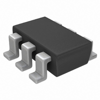
MOSFET P-CHAN DUAL 20V SSOT6

FDC6306P

Manufacturer Part Number
FDC6306P
Description
MOSFET P-CHAN DUAL 20V SSOT6
Manufacturer
Fairchild Semiconductor
Series
PowerTrench®r
Datasheet

Specifications of FDC6306P

Fet Type
2 P-Channel (Dual)
Fet Feature
Logic Level Gate
Rds On (max) @ Id, Vgs
170 mOhm @ 1.9A, 4.5V
Drain To Source Voltage (vdss)
20V
Current - Continuous Drain (id) @ 25° C
1.9A
Vgs(th) (max) @ Id
1.5V @ 250µA
Gate Charge (qg) @ Vgs
4.2nC @ 4.5V
Input Capacitance (ciss) @ Vds
441pF @ 10V
Power - Max
700mW
Mounting Type
Surface Mount
Package / Case
6-SSOT, SuperSOT-6
Configuration
Dual
Transistor Polarity
P-Channel
Resistance Drain-source Rds (on)
0.17 Ohm @ 4.5 V
Forward Transconductance Gfs (max / Min)
4 S
Drain-source Breakdown Voltage
20 V
Gate-source Breakdown Voltage
+/- 8 V
Continuous Drain Current
1.9 A
Power Dissipation
960 mW
Maximum Operating Temperature
+ 150 C
Mounting Style
SMD/SMT
Minimum Operating Temperature
- 55 C
Module Configuration
Dual
Continuous Drain Current Id
-1.9A
Drain Source Voltage Vds
-20V
On Resistance Rds(on)
127mohm
Rds(on) Test Voltage Vgs
-4.5V
Rohs Compliant
Yes
Lead Free Status / RoHS Status
Lead free / RoHS Compliant
Other names
FDC6306PTR

Available stocks

Company
Part Number
Manufacturer
Quantity
Price
Part Number:
FDC6306P
Manufacturer:
FSC
Quantity:
60 000
Part Number:
FDC6306P
Manufacturer:
FAIRCHILD
Quantity:
30 000
Part Number:
FDC6306P
Manufacturer:
FAIRCHILD/仙童
Quantity:
20 000
Part Number:
FDC6306P
0
Company:
Part Number:
FDC6306P
Quantity:
14 683
Part Number:
FDC6306P-NL
Manufacturer:
FAIRCHILD/仙童
Quantity:
20 000
Part Number:
FDC6306P_NL
Manufacturer:
FAIRCHILD/仙童
Quantity:
20 000
1999 Fairchild Semiconductor Corporation
General Description
These P-Channel 2.5V specified MOSFETs are produced
using Fairchild Semiconductor's advanced PowerTrench
process that has been especially tailored to minimize
on-state resistance and yet maintain low gate charge for
superior switching performance.
These devices have been designed to offer exceptional
power dissipation in a very small footprint for applications
where the bigger more expensive SO-8 and TSSOP-8
packages are impractical.
Applications
FDC6306P
Dual P-Channel 2.5V Specified PowerTrench
Absolute Maximum Ratings
V
V
I
P
T
Thermal Characteristics
R
R
Package Outlines and Ordering Information
Symbol
D
Load switch
Battery protection
Power management
DSS
GSS
D
J
, T
JA
JC
Device Marking
stg
SuperSOT
.
306
Drain-Source Voltage
Gate-Source Voltage
Drain Current
Power Dissipation for Single Operation
Operating and Storage Junction Temperature Range
Thermal Resistance, Junction-to-Ambient
Thermal Resistance, Junction-to-Case
D1
S1
TM
-6
D2
- Pulsed
- Continuous
G1
FDC6306P
Parameter
Device
S2
G2
T
A
= 25°C unless otherwise noted
Reel Size
7’’
(Note 1a)
(Note 1a)
(Note 1b)
(Note 1c)
(Note 1a)
(Note 1)
Features
than standard SO-8); low profile (1mm thick).
-1.9 A, -20 V. R
Low gate charge (3 nC typical).
Fast switching speed.
low R
SuperSOT TM -6 package: small footprint (72% smaller
High performance trench technology for extremely
DS(ON)
MOSFET
.
4
5
6
R
Tape Width
DS(on)
DS(on)
-55 to +150
Ratings
8mm
= 0.170
0.96
= 0.250
-1.9
130
-20
0.9
0.7
60
-5
8
@ V
@ V
3
1
2
February 1999
GS
GS
Quantity
3000 units
= -2.5 V
= -4.5 V
Units
C/W
C/W
FDC6306P Rev. C
W
V
V
A
C

Related parts for FDC6306P

FDC6306P Summary of contents

Page 1

... A Parameter (Note 1a) (Note 1a) (Note 1b) (Note 1c) (Note 1a) (Note 1) Device Reel Size FDC6306P 7’’ February 1999 = 0.170 @ V = -4.5 V DS(on 0.250 @ V = -2.5 V DS(on Ratings Units - -1 0.96 W 0.9 0.7 -55 to +150 C 130 C/W 60 C/W Tape Width Quantity 8mm 3000 units FDC6306P Rev. C ...

Page 2

... Min Typ Max Units -20 V -18 mV 100 nA -100 nA -0.4 -0.9 -1 mV/ C 0.127 0.170 0.182 0.270 0.194 0.250 - 441 pF 127 4.2 nC 0.7 nC 0.8 nC -0.8 A -0.8 -1 180 C/W when 2 mounted on a 0.0015 in pad of 2 oz. copper. FDC6306P Rev ...

Page 3

... Figure 6. Body Diode Forward Voltage Variation with Source Current = - -3.0V -3.5V -4.0V -4. DRAIN CURRENT ( - 25° 25° GATE TO SOURCE VOLT 125° °C -55°C 0.2 0.4 0.6 0 BODY DIODE FORWARD VOLT AGE (V) SD and Temperature. FDC6306P Rev 1.4 ...

Page 4

... Transient themal response will change depending on the circuit board design. C iss C oss C rss 0 DRAIN T O SOURCE VOLTAGE (V) DS SINGLE PULSE R =180°C 25° 100 SINGLE PULSE TIME (SEC) Power Dissipation. R ( 180 °C/W JA P(pk ( Duty Cycle 100 300 FDC6306P Rev 300 ...

Page 5

... TRADEMARKS The following are registered and unregistered trademarks Fairchild Semiconductor owns or is authorized to use and is not intended exhaustive list of all such trademarks. ACEx™ CoolFET™ CROSSVOLT™ CMOS FACT™ FACT Quiet Series™ ® FAST FASTr™ GTO™ ...

Related keywords