SI1563DH-T1-E3 Vishay, SI1563DH-T1-E3 Datasheet - Page 6
SI1563DH-T1-E3
Manufacturer Part Number
SI1563DH-T1-E3
Description
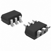
MOSFET N/P-CH 20V SC70-6
Manufacturer
Vishay
Series
TrenchFET®r
Type
Power MOSFETr
Datasheet
1.SI1563DH-T1-E3.pdf
(9 pages)
Specifications of SI1563DH-T1-E3
Transistor Polarity
N and P-Channel
Fet Type
N and P-Channel
Fet Feature
Logic Level Gate
Rds On (max) @ Id, Vgs
280 mOhm @ 1.13A, 4.5V
Drain To Source Voltage (vdss)
20V
Current - Continuous Drain (id) @ 25° C
1.13A, 880mA
Vgs(th) (max) @ Id
1V @ 100µA
Gate Charge (qg) @ Vgs
2nC @ 4.5V
Power - Max
570mW
Mounting Type
Surface Mount
Package / Case
SC-70-6, SC-88, SOT-363
Minimum Operating Temperature
- 55 C
Configuration
Dual
Resistance Drain-source Rds (on)
0.28 Ohm @ 4.5 V @ N Channel
Drain-source Breakdown Voltage
20 V
Gate-source Breakdown Voltage
+/- 8 V
Continuous Drain Current
1.13 A @ N Channel or 0.88 A @ P Channel
Power Dissipation
570 mW
Maximum Operating Temperature
+ 150 C
Mounting Style
SMD/SMT
Continuous Drain Current Id
1.13A
Drain Source Voltage Vds
20V
On Resistance Rds(on)
490mohm
Rds(on) Test Voltage Vgs
4.5V
Threshold Voltage Vgs Typ
1V
Number Of Elements
2
Polarity
N/P
Channel Mode
Enhancement
Drain-source On-volt
20V
Gate-source Voltage (max)
±8V
Output Power (max)
Not RequiredW
Frequency (max)
Not RequiredMHz
Noise Figure
Not RequireddB
Power Gain
Not RequireddB
Drain Efficiency
Not Required%
Operating Temp Range
-55C to 150C
Operating Temperature Classification
Military
Mounting
Surface Mount
Pin Count
6
Package Type
SOT-363
Lead Free Status / RoHS Status
Lead free / RoHS Compliant
Lead Free Status / RoHS Status
Lead free / RoHS Compliant, Lead free / RoHS Compliant
Other names
SI1563DH-T1-E3TR
Available stocks
Company
Part Number
Manufacturer
Quantity
Price
Company:

Part Number:
SI1563DH-T1-E3
Manufacturer:
Vishay/Siliconix
Quantity:
67 465


Si1563DH
Vishay Siliconix
P-CHANNEL TYPICAL CHARACTERISTICS 25 °C, unless otherwise noted
www.vishay.com
6
1.6
1.2
0.8
0.4
0.0
3.0
2.5
2.0
1.5
1.0
0.5
0.0
5
4
3
2
1
0
0.0
0.0
0
V
thru 3.5 V
GS
= 5 V
V
I
D
DS
0.5
On-Resistance vs. Drain Current
= 0.9 A
0.3
= 10 V
V
DS
1
Output Characteristics
Q
V
g
- Drain-to-Source Voltage (V)
V
1.0
GS
I
- Total Gate Charge (nC)
D
GS
- Drain Current (A)
Gate Charge
= 1.8 V
0.6
= 2.5 V
1.5
2
0.9
2.0
3
V
GS
1.2
2.5
= 4.5 V
1.5 V
2.5 V
2 V
1 V
3 V
3.0
1.5
4
160
120
3.0
2.5
2.0
1.5
1.0
0.5
0.0
1.6
1.4
1.2
1.0
0.8
0.6
80
40
0
- 50
0.0
0
C
rss
On-Resistance vs. Junction Temperature
V
I
D
- 25
GS
0.5
= 0.88 A
2
= 4.5 V
V
V
GS
DS
Transfer Characteristics
0
T
1.0
J
- Drain-to-Source Voltage (V)
- Junction Temperature (°C)
- Gate-to-Source Voltage (V)
4
25
Capacitance
C
C
1.5
oss
iss
S10-1054-Rev. B, 03-May-10
50
6
T
Document Number: 71963
C
2.0
25 °C
= - 55 °C
75
8
2.5
100
125 °C
10
3.0
125
150
3.5
12
Related parts for SI1563DH-T1-E3
Image
Part Number
Description
Manufacturer
Datasheet
Request
R

Part Number:
Description:
N/P-Ch SC-70-6 (SOT-363) 20V 280/490mohm @ 4.5V
Manufacturer:
Vishay

Part Number:
Description:
Complementary 20-V (D-S) Low-Threshold MOSFET
Manufacturer:
Vishay Siliconix
Datasheet:
Part Number:
Description:
MOSFET 20V 1.28/1.0A 0.48W
Manufacturer:
Vishay/Siliconix
Datasheet:
Part Number:
Description:
357-036-542-201 CARDEDGE 36POS DL .156 BLK LOPRO
Manufacturer:
Vishay
Datasheet:
Part Number:
Description:
357-036-542-201 CARDEDGE 36POS DL .156 BLK LOPRO
Manufacturer:
Vishay
Datasheet:
Part Number:
Description:
357-036-542-201 CARDEDGE 36POS DL .156 BLK LOPRO
Manufacturer:
Vishay
Datasheet:
Part Number:
Description:
357-036-542-201 CARDEDGE 36POS DL .156 BLK LOPRO
Manufacturer:
Vishay
Datasheet:
Part Number:
Description:
357-036-542-201 CARDEDGE 36POS DL .156 BLK LOPRO
Manufacturer:
Vishay
Datasheet:
Part Number:
Description:
357-036-542-201 CARDEDGE 36POS DL .156 BLK LOPRO
Manufacturer:
Vishay
Datasheet:
Part Number:
Description:
357-036-542-201 CARDEDGE 36POS DL .156 BLK LOPRO
Manufacturer:
Vishay
Datasheet:
Part Number:
Description:
357-036-542-201 CARDEDGE 36POS DL .156 BLK LOPRO
Manufacturer:
Vishay
Datasheet:
Part Number:
Description:
357-036-542-201 CARDEDGE 36POS DL .156 BLK LOPRO
Manufacturer:
Vishay
Datasheet:
Part Number:
Description:
357-036-542-201 CARDEDGE 36POS DL .156 BLK LOPRO
Manufacturer:
Vishay
Datasheet:
Part Number:
Description:
357-036-542-201 CARDEDGE 36POS DL .156 BLK LOPRO
Manufacturer:
Vishay
Datasheet:
Part Number:
Description:
357-036-542-201 CARDEDGE 36POS DL .156 BLK LOPRO
Manufacturer:
Vishay
Datasheet: