SIA511DJ-T1-GE3 Vishay, SIA511DJ-T1-GE3 Datasheet - Page 2
SIA511DJ-T1-GE3
Manufacturer Part Number
SIA511DJ-T1-GE3
Description
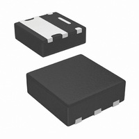
MOSFET N/P-CH 12V PWRPAK SC70-6
Manufacturer
Vishay
Datasheet
1.SIA511DJ-T1-GE3.pdf
(12 pages)
Specifications of SIA511DJ-T1-GE3
Transistor Polarity
N and P-Channel
Fet Type
N and P-Channel
Fet Feature
Logic Level Gate
Rds On (max) @ Id, Vgs
40 mOhm @ 4.2A, 4.5V
Drain To Source Voltage (vdss)
12V
Current - Continuous Drain (id) @ 25° C
4.5A, 4.3A
Vgs(th) (max) @ Id
1V @ 250µA
Gate Charge (qg) @ Vgs
12nC @ 8V
Input Capacitance (ciss) @ Vds
400pF @ 6V
Power - Max
1.9W
Mounting Type
Surface Mount
Package / Case
PowerPAK® SC-70-6 Dual
Minimum Operating Temperature
- 55 C
Configuration
Dual
Resistance Drain-source Rds (on)
0.04 Ohm @ 4.5 V @ N Channel
Forward Transconductance Gfs (max / Min)
13 S, 9 S
Drain-source Breakdown Voltage
12 V
Gate-source Breakdown Voltage
+/- 8 V
Continuous Drain Current
4.5 A @ N Channel or 4.3 A @ P Channel
Power Dissipation
1900 mW
Maximum Operating Temperature
+ 150 C
Mounting Style
SMD/SMT
Continuous Drain Current Id
4.5A
Drain Source Voltage Vds
12V
On Resistance Rds(on)
33mohm
Rds(on) Test Voltage Vgs
4.5V
Threshold Voltage Vgs Typ
1V
Lead Free Status / RoHS Status
Lead free / RoHS Compliant
Lead Free Status / RoHS Status
Lead free / RoHS Compliant, Lead free / RoHS Compliant
Other names
SIA511DJ-T1-GE3TR


SiA511DJ
Vishay Siliconix
Notes:
a. Guaranteed by design, not subject to production testing.
b. Pulse test; pulse width ≤ 300 µs, duty cycle ≤ 2 %.
www.vishay.com
2
SPECIFICATIONS T
Parameter
Static
Drain-Source Breakdown Voltage
V
V
Gate Threshold Voltage
Gate-Body Leakage
Zero Gate Voltage Drain Current
On-State Drain Current
Drain-Source On-State Resistance
Forward Transconductance
Dynamic
Input Capacitance
Output Capacitance
Reverse Transfer Capacitance
Total Gate Charge
Gate-Source Charge
Gate-Drain Charge
Gate Resistance
DS
GS(th)
Temperature Coefficient
Temperature Coefficient
a
b
b
J
= 25 °C, unless otherwise noted
b
ΔV
Symbol
ΔV
R
V
GS(th)
I
I
I
C
V
DS(on)
C
GS(th)
D(on)
C
Q
Q
GSS
DSS
DS
g
Q
R
DS
oss
iss
rss
gd
fs
gs
g
g
/T
/T
J
J
V
New Product
V
V
DS
V
V
V
DS
DS
V
V
DS
DS
DS
DS
DS
= - 6 V, V
= - 6 V, V
= - 12 V, V
V
V
V
V
V
V
= 12 V, V
V
= 6 V, V
V
= - 6 V, V
V
V
V
V
V
V
V
DS
GS
GS
GS
= 6 V, V
= 6 V, V
DS
V
V
DS
GS
DS
DS
GS
DS
DS
GS
GS
GS
DS
DS
≤ - 5 V, V
= - 4.5 V, I
= - 2.5 V, I
= - 1.8 V, I
= V
= - 10 V, I
= 0 V, I
= V
= - 12 V, V
= 0 V, V
= 0 V, I
≥ 5 V, V
= 4.5 V, I
= 2.5 V, I
= 1.8 V, I
I
I
= 12 V, V
= 10 V, I
D
D
I
I
N-Channel
N-Channel
D
D
P-Channel
P-Channel
GS
f = 1 MHz
GS
GS
Test Conditions
= - 250 µA
= - 250 µA
GS
GS
GS
= 250 µA
= 250 µA
GS
GS
GS
GS
, I
= - 4.5 V, I
, I
= 4.5 V, I
= - 8 V, I
D
= 0 V, f = 1 MHz
= 8 V, I
D
= 0 V, T
D
= 0 V, f = 1 MHz
D
= 0 V, T
GS
GS
GS
= - 250 µA
= - 250 µA
D
D
= 250 µA
D
D
D
D
D
D
= 250 µA
GS
GS
= 4.2 A
= - 3.3 A
= 4.2 A
= - 3.3 A
= 3.8 A
= - 2.8 A
= 1.6 A
= - 0.7 A
= 4.5 V
= - 4.5 V
= ± 8 V
= 0 V
= 0 V
D
D
J
D
J
D
= 5.5 A
= 55 °C
= - 4.3 A
= 5.5 A
= 55 °C
= - 4.3 A
N-Ch
P-Ch
N-Ch
P-Ch
N-Ch
P-Ch
N-Ch
P-Ch
N-Ch
P-Ch
N-Ch
P-Ch
N-Ch
P-Ch
N-Ch
P-Ch
N-Ch
P-Ch
N-Ch
P-Ch
N-Ch
P-Ch
N-Ch
P-Ch
N-Ch
P-Ch
N-Ch
P-Ch
N-Ch
P-Ch
N-Ch
P-Ch
N-Ch
P-Ch
N-Ch
P-Ch
N-Ch
P-Ch
N-Ch
P-Ch
Min.
- 0.4
- 12
0.4
- 8
12
15
S-80436-Rev. B, 03-Mar-08
Document Number: 74592
0.033
0.058
0.039
0.082
0.051
0.111
Typ.
- 2.8
400
400
120
140
100
2.1
7.5
4.5
0.6
0.8
0.8
1.4
2.5
12
- 7
13
70
9
8
5
7
± 100
± 100
0.040
0.070
0.048
0.100
0.063
0.140
Max.
- 10
6.8
7.5
- 1
- 1
10
12
12
1
1
mV/°C
Unit
nC
nA
µA
pF
V
V
A
Ω
S
Ω
Related parts for SIA511DJ-T1-GE3
Image
Part Number
Description
Manufacturer
Datasheet
Request
R

Part Number:
Description:
MOSFET 12V 4.5A 6.5W
Manufacturer:
Vishay/Siliconix
Datasheet:

Part Number:
Description:
N- And P-channel 12-v D-s Mosfet
Manufacturer:
Vishay
Datasheet:
Part Number:
Description:
357-036-542-201 CARDEDGE 36POS DL .156 BLK LOPRO
Manufacturer:
Vishay
Datasheet:
Part Number:
Description:
357-036-542-201 CARDEDGE 36POS DL .156 BLK LOPRO
Manufacturer:
Vishay
Datasheet:
Part Number:
Description:
357-036-542-201 CARDEDGE 36POS DL .156 BLK LOPRO
Manufacturer:
Vishay
Datasheet:
Part Number:
Description:
357-036-542-201 CARDEDGE 36POS DL .156 BLK LOPRO
Manufacturer:
Vishay
Datasheet:
Part Number:
Description:
357-036-542-201 CARDEDGE 36POS DL .156 BLK LOPRO
Manufacturer:
Vishay
Datasheet:
Part Number:
Description:
357-036-542-201 CARDEDGE 36POS DL .156 BLK LOPRO
Manufacturer:
Vishay
Datasheet:
Part Number:
Description:
357-036-542-201 CARDEDGE 36POS DL .156 BLK LOPRO
Manufacturer:
Vishay
Datasheet:
Part Number:
Description:
357-036-542-201 CARDEDGE 36POS DL .156 BLK LOPRO
Manufacturer:
Vishay
Datasheet:
Part Number:
Description:
357-036-542-201 CARDEDGE 36POS DL .156 BLK LOPRO
Manufacturer:
Vishay
Datasheet:
Part Number:
Description:
357-036-542-201 CARDEDGE 36POS DL .156 BLK LOPRO
Manufacturer:
Vishay
Datasheet:
Part Number:
Description:
357-036-542-201 CARDEDGE 36POS DL .156 BLK LOPRO
Manufacturer:
Vishay
Datasheet:
Part Number:
Description:
357-036-542-201 CARDEDGE 36POS DL .156 BLK LOPRO
Manufacturer:
Vishay
Datasheet:
Part Number:
Description:
357-036-542-201 CARDEDGE 36POS DL .156 BLK LOPRO
Manufacturer:
Vishay
Datasheet: