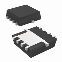
SI7913DN-T1-E3 Vishay, SI7913DN-T1-E3 Datasheet - Page 3

SI7913DN-T1-E3
Manufacturer Part Number
SI7913DN-T1-E3
Description
MOSFET DUAL P-CH 20V 1212-8
Manufacturer
Vishay
Series
TrenchFET®r
Specifications of SI7913DN-T1-E3
Fet Type
2 P-Channel (Dual)
Fet Feature
Logic Level Gate
Rds On (max) @ Id, Vgs
37 mOhm @ 7.4A, 4.5V
Drain To Source Voltage (vdss)
20V
Current - Continuous Drain (id) @ 25° C
5A
Vgs(th) (max) @ Id
1V @ 250µA
Gate Charge (qg) @ Vgs
24nC @ 4.5V
Power - Max
1.3W
Mounting Type
Surface Mount
Package / Case
PowerPAK® 1212-8 Dual
Transistor Polarity
P Channel
Continuous Drain Current Id
-7.4A
Drain Source Voltage Vds
-20V
On Resistance Rds(on)
66mohm
Rds(on) Test Voltage Vgs
8V
Threshold Voltage Vgs Typ
-1V
Lead Free Status / RoHS Status
Lead free / RoHS Compliant
Other names
SI7913DN-T1-E3TR
TYPICAL CHARACTERISTICS 25 °C, unless otherwise noted
Document Number: 72615
S-83050-Rev. C, 29-Dec-08
0.10
0.08
0.06
0.04
0.02
0.00
20
10
5
4
3
2
1
0
1
0.0
0
0
V
Source-Drain Diode Forward Voltage
V
I
GS
D
DS
On-Resistance vs. Drain Current
0.2
= 7.4 A
= 1.8 V
= 10 V
4
4
V
SD
Q
g
- Source-to-Drain Voltage (V)
- Total Gate Charge (nC)
0.4
T
I
D
J
Gate Charge
= 150 °C
- Drain Current (A)
8
8
0.6
12
12
0.8
V
V
T
GS
GS
J
16
16
= 25 °C
= 2.5 V
= 4.5 V
1.0
20
20
1.2
2100
1800
1500
1200
0.10
0.08
0.06
0.04
0.02
0.00
900
600
300
1.6
1.4
1.2
1.0
0.8
0.6
0
- 50
0
0
On-Resistance vs. Gate-to-Source Voltage
On-Resistance vs. Junction Temperature
I
D
- 25
C
V
I
= 1.5 A
D
rss
GS
= 7.4 A
1
4
= 4.5 V
V
V
T
GS
0
DS
J
- Junction Temperature (°C)
- Gate-to-Source Voltage (V)
C
- Drain-to-Source Voltage (V)
oss
25
Capacitance
2
8
I
D
= 7.4 A
50
Vishay Siliconix
C
12
3
iss
75
Si7913DN
www.vishay.com
100
16
4
125
150
20
5
3


