NTJD4152PT1G ON Semiconductor, NTJD4152PT1G Datasheet
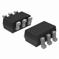
MOSFET 2P-CH 20V 880MA SOT-363

NTJD4152PT1G

Manufacturer Part Number
NTJD4152PT1G
Description
MOSFET 2P-CH 20V 880MA SOT-363
Manufacturer
ON Semiconductor
Type
Small Signalr
Datasheets

Specifications of NTJD4152PT1G

Fet Type
2 P-Channel (Dual)
Fet Feature
Logic Level Gate
Rds On (max) @ Id, Vgs
260 mOhm @ 880mA, 4.5V
Drain To Source Voltage (vdss)
20V
Current - Continuous Drain (id) @ 25° C
880mA
Vgs(th) (max) @ Id
450mV @ 250µA
Gate Charge (qg) @ Vgs
2.2nC @ 4.5V
Input Capacitance (ciss) @ Vds
155pF @ 20V
Power - Max
272mW
Mounting Type
Surface Mount
Package / Case
SC-70-6, SC-88, SOT-363
Configuration
Dual
Transistor Polarity
P-Channel
Resistance Drain-source Rds (on)
0.26 Ohm @ 4.5 V
Forward Transconductance Gfs (max / Min)
3 S
Drain-source Breakdown Voltage
20 V
Gate-source Breakdown Voltage
+/- 12 V
Continuous Drain Current
0.88 A
Power Dissipation
272 mW
Maximum Operating Temperature
+ 150 C
Mounting Style
SMD/SMT
Minimum Operating Temperature
- 55 C
Module Configuration
Dual
Continuous Drain Current Id
880mA
Drain Source Voltage Vds
-20V
On Resistance Rds(on)
215mohm
Rds(on) Test Voltage Vgs
-4.5V
Rohs Compliant
Yes
Number Of Elements
2
Polarity
P
Channel Mode
Enhancement
Drain-source On-res
0.26Ohm
Drain-source On-volt
20V
Gate-source Voltage (max)
±12V
Operating Temp Range
-55C to 150C
Operating Temperature Classification
Military
Mounting
Surface Mount
Pin Count
6
Package Type
SC-88
Lead Free Status / RoHS Status
Lead free / RoHS Compliant
Other names
NTJD4152PT1GOSTR

Available stocks

Company
Part Number
Manufacturer
Quantity
Price
Part Number:
NTJD4152PT1G
Manufacturer:
ON
Quantity:
36 000
Part Number:
NTJD4152PT1G
Manufacturer:
ON
Quantity:
3 000
Part Number:
NTJD4152PT1G
Manufacturer:
ON
Quantity:
30 000
Part Number:
NTJD4152PT1G
Manufacturer:
ON/安森美
Quantity:
20 000
Part Number:
NTJD4152PT1G
0
Company:
Part Number:
NTJD4152PT1G
Quantity:
3 451
Company:
Part Number:
NTJD4152PT1G
Quantity:
4 500
Company:
Part Number:
NTJD4152PT1G
Quantity:
15 000
NSQA6V8AW5T2 Series
Transient Voltage Suppressor
ESD Protection Diode with Low Clamping
Voltage
designed for applications requiring transient overvoltage protection. It
is intended for use in sensitive equipment such as computers, printers,
business machines, communication systems, medical equipment, and
other applications. Its integrated design provides very effective and
reliable protection for four separate lines using only one package.
These devices are ideal for situations where board space is at a premium.
Features
Benefits
Typical Applications
Stresses exceeding Maximum Ratings may damage the device. Maximum
Ratings are stress ratings only. Functional operation above the Recommended
Operating Conditions is not implied. Extended exposure to stresses above the
Recommended Operating Conditions may affect device reliability.
1. Non−repetitive current pulse per Figure 6.
2. Only 1 diode under power. For all 4 diodes under power, P
See Application Note AND8308/D for further description of survivability specs.
© Semiconductor Components Industries, LLC, 2009
September, 2009 − Rev. 5
MAXIMUM RATINGS
Peak Power Dissipation
Steady State Power − 1 Diode (Note
Thermal Resistance −
Operating Junction Temperature
Storage Temperature Range
Lead Solder Temperature − Maximum
IEC ^1000−4−2 (ESD)
This integrated transient voltage suppressor device (TVS) is
Low Clamping Voltage
Small SC−88A SMT Package
Stand Off Voltage: 5 V
Low Leakage Current < 1 mA
Four Separate Unidirectional Configurations for Protection
ESD Protection: IEC61000−4−2: Level 4
Pb−Free Packages are Available
Provides Protection for ESD Industry Standards: IEC 61000, HBM
Minimize Power Consumption of the System
Minimize PCB Board Space
Instrumentation Equipment
Serial and Parallel Ports
Microprocessor Based Equipment
Notebooks, Desktops, Servers
Cellular and Portable Equipment
Mounted on FR4 board with min pad.
8
Waveform (Note 1)
2)
Junction−to−Ambient
Above 25°C, Derate
Range
10 Seconds Duration
20 msec Double Exponential
Rating
MILSTD 883C − Method 3015−6: Class 3
(T
A
= 25°C unless otherwise noted)
Contact
Symbol
R
P
T
P
T
T
qJA
stg
PK
D
J
L
−40 to +125
−55 to +150
Value
$8.0
3.05
380
327
260
20
D
will be 25%.
1
mW/°C
°C/W
Unit
mW
°C
°C
°C
kV
W
†For information on tape and reel specifications,
NSQA6V8AW5T2
NSQA6V8AW5T2G
NSQA12VAW5T2
NSQA12VAW5T2G
including part orientation and tape sizes, please
refer to our Tape and Reel Packaging Specifications
Brochure, BRD8011/D.
(Note: Microdot may be in either location)
Device
x
M
G
1
2
3
ORDERING INFORMATION
MARKING DIAGRAM
http://onsemi.com
= H for NSQA6V8AW5T2
= Date Code
= Pb−Free Package
SC−88A/SOT−323
X for NSQA12VAW5T2
4
1
CASE 419A
(Pb−Free)
(Pb−Free)
Package
SC−88A
SC−88A
SC−88A
SC−88A
6x MG
2
Publication Order Number:
G
5
3
NSQA6V8AW5T2/D
3000/Tape & Reel
3000/Tape & Reel
3000/Tape & Reel
3000/Tape & Reel
Shipping
5
4

Related parts for NTJD4152PT1G

NTJD4152PT1G Summary of contents

Page 1

NSQA6V8AW5T2 Series Transient Voltage Suppressor ESD Protection Diode with Low Clamping Voltage This integrated transient voltage suppressor device (TVS) is designed for applications requiring transient overvoltage protection intended for use in sensitive equipment such as computers, printers, business ...

Page 2

ELECTRICAL CHARACTERISTICS (T = 25°C unless otherwise noted) A Symbol Parameter I Maximum Reverse Peak Pulse Current PP V Clamping Voltage @ Working Peak Reverse Voltage RWM I Maximum Reverse Leakage Current @ ...

Page 3

Figure 1. ESD Clamping Voltage Screenshot Positive 8 kV Contact per IEC61000−4−2 Figure 2. ESD Clamping Voltage Screenshot Negative 8 kV Contact per IEC61000−4−2 http://onsemi.com 3 ...

Page 4

... ON Semiconductor has developed a way to examine the entire voltage waveform across the ESD protection diode over the time domain of an ESD pulse in the form of an oscilloscope screenshot, which can be found on the datasheets for all ESD protection diodes ...

Page 5

TIME (ms) Figure 6. Pulse Width 0.16 0.14 0.12 0.10 0.08 0.06 0.04 0.02 0 −60 −40 − TEMPERATURE (°C) Figure 8. Reverse Leakage versus Temperature 1 0.1 0.01 0.001 ...

Page 6

... Pb−Free strategy and soldering details, please download the ON Semiconductor Soldering and Mounting Techniques Reference Manual, SOLDERRM/D. ON Semiconductor and are registered trademarks of Semiconductor Components Industries, LLC (SCILLC). SCILLC reserves the right to make changes without further notice to any products herein ...

Related keywords