NTHD4102PT1G ON Semiconductor, NTHD4102PT1G Datasheet
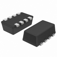
MOSFET PWR P-CH DUAL20V CHIPFET

NTHD4102PT1G

Manufacturer Part Number
NTHD4102PT1G
Description
MOSFET PWR P-CH DUAL20V CHIPFET
Manufacturer
ON Semiconductor
Datasheet

Specifications of NTHD4102PT1G

Fet Type
2 P-Channel (Dual)
Fet Feature
Logic Level Gate
Rds On (max) @ Id, Vgs
80 mOhm @ 2.9A, 4.5V
Drain To Source Voltage (vdss)
20V
Current - Continuous Drain (id) @ 25° C
2.9A
Vgs(th) (max) @ Id
1.5V @ 250µA
Gate Charge (qg) @ Vgs
8.6nC @ 4.5V
Input Capacitance (ciss) @ Vds
750pF @ 16V
Power - Max
1.1W
Mounting Type
Surface Mount
Package / Case
8-ChipFET™
Lead Free Status / RoHS Status
Lead free / RoHS Compliant
Other names
NTHD4102PT1GOS
NTHD4102PT1GOS
NTHD4102PT1GOSTR

Available stocks

Company
Part Number
Manufacturer
Quantity
Price
Part Number:
NTHD4102PT1G
Manufacturer:
ON
Quantity:
5 950
Part Number:
NTHD4102PT1G
Manufacturer:
ON/安森美
Quantity:
20 000
Company:
Part Number:
NTHD4102PT1G
Quantity:
4 500
NTHD4102P
Power MOSFET
−20 V, −4.1 A, Dual P−Channel ChipFETt
Features
Applications
Maximum ratings are those values beyond which device damage can occur.
Maximum ratings applied to the device are individual stress limit values (not
normal operating conditions) and are not valid simultaneously. If these limits are
exceeded, device functional operation is not implied, damage may occur and
reliability may be affected.
1. Surface mounted on FR4 board using 1 in sq pad size (Cu area = 1.127 in sq
MAXIMUM RATINGS
© Semiconductor Components Industries, LLC, 2005
November, 2005 − Rev. 5
THERMAL RESISTANCE RATINGS
Drain−to−Source Voltage
Gate−to−Source Voltage
Continuous Drain
Current (Note 1)
Power Dissipation
(Note 1)
Pulsed Drain
Current
Operating Junction and Storage Temperature
Source Current (Body Diode)
Lead Temperature for Soldering
Purposes (1/8” from case for 10 s)
Junction−to−Ambient, Steady State (Note 1)
Junction−to−Ambient, t ≤ 10s (Note 1)
Environments such as Portable Electronics
Voltages are not Required
Migration to Lower Levels using the same Basic Topology
Portable Equipment such as MP3 Players, Cell Phones, and PDAs
Offers an Ultra Low R
Miniature ChipFET Package 40% Smaller Footprint than TSOP−6
Low Profile (<1.1 mm) Allows it to Fit Easily into Extremely Thin
Simplifies Circuit Design since Additional Boost Circuits for Gate
Operated at Standard Logic Level Gate Drive, Facilitating Future
Pb−Free Package is Available
Optimized for Battery and Load Management Applications in
Charge Control in Battery Chargers
Buck and Boost Converters
[1 oz] including traces)
Parameter
Parameter
Steady State
Steady State
(T
t ≤ 10 s
t ≤ 10 s
J
DS(ON)
= 25°C unless otherwise noted)
tp = 10 ms
Solution in the ChipFET Package
T
T
T
T
A
A
A
A
= 25°C
= 85°C
= 25°C
= 25°C
Symbol
Symbol
V
T
R
V
I
P
T
STG
T
DSS
I
DM
I
qJA
GS
D
S
J
D
L
,
−55 to
Value
−13.8
"8.0
−2.9
−2.1
−4.1
−1.1
Max
−20
150
260
113
1.1
2.1
60
1
°C/W
Unit
Unit
°C
°C
W
V
V
A
A
A
G
†For information on tape and reel specifications,
NTHD4102PT1
NTHD4102PT1G
1
including part orientation and tape sizes, please
refer to our Tape and Reel Packaging Specifications
Brochure, BRD8011/D.
D
D
D
D
V
P−Channel MOSFET
−20 V
1
1
2
2
CONNECTIONS
(BR)DSS
Device
8
7
6
5
ORDERING INFORMATION
PIN
S
C7 = Specific Device Code
M
G
1
http://onsemi.com
= Month Code
= Pb−Free Package
D
1
2
3
4
64 mW @ −4.5 V
120 mW @ −1.8 V
85 mW @ −2.5 V
1
(Pb−Free)
Package
ChipFET
ChipFET
R
S
G
S
G
DS(ON)
1
2
1
2
Publication Order Number:
G
2
1
2
3
4
TYP
P−Channel MOSFET
CASE 1206A
MARKING
DIAGRAM
ChipFET
STYLE 2
3000/Tape & Reel
3000/Tape & Reel
NTHD4102P/D
Shipping
S
2
I
D
−4.1 A
MAX
D
2
8
7
6
5

Related parts for NTHD4102PT1G

NTHD4102PT1G Summary of contents

Page 1

... S °C T 260 L Symbol Max Unit °C/W 113 Device R qJA 60 NTHD4102PT1 NTHD4102PT1G †For information on tape and reel specifications, including part orientation and tape sizes, please refer to our Tape and Reel Packaging Specifications Brochure, BRD8011/D. 1 http://onsemi.com R TYP I MAX DS(ON −4 −2.5 V −4.1 A 120 mW @ − ...

Page 2

ELECTRICAL CHARACTERISTICS (T Characteristic OFF CHARACTERISTICS Drain−to−Source Breakdown Voltage Drain−to−Source Breakdown Voltage Temperature Coefficient Zero Gate Voltage Drain Current Gate−to−Source Leakage Current ON CHARACTERISTICS (Note 2) Gate Threshold Voltage Gate Threshold Temperature Coefficient Drain−to−Source On Resistance Forward Transconductance CHARGES, CAPACITANCES, ...

Page 3

TYPICAL PERFORMANCE CURVES − −2 −V , DRAIN−TO−SOURCE VOLTAGE (VOLTS) DS Figure 1. On−Region Characteristics 0.2 0.18 ...

Page 4

TYPICAL PERFORMANCE CURVES 1000 900 800 700 600 500 400 300 200 100 C rss −V − GATE−TO−SOURCE OR DRAIN−TO−SOURCE VOLTAGE (VOLTS) Figure 6. Capacitance Variation 1000 V = −10 ...

Page 5

... SCALE 20:1 0.026 Basic *For additional information on our Pb−Free strategy and soldering details, please download the ON Semiconductor Soldering and Mounting Techniques Reference Manual, SOLDERRM/D. NTHD4102P PACKAGE DIMENSIONS ChipFET] CASE 1206A−03 ISSUE G NOTES: 1. DIMENSIONING AND TOLERANCING PER ANSI Y14.5M, 1982. ...

Page 6

... Fax: 480−829−7709 or 800−344−3867 Toll Free USA/Canada Email: orderlit@onsemi.com NTHD4102P N. American Technical Support: 800−282−9855 Toll Free USA/Canada Japan: ON Semiconductor, Japan Customer Focus Center 2−9−1 Kamimeguro, Meguro−ku, Tokyo, Japan 153−0051 Phone: 81−3−5773−3850 http://onsemi.com 6 ON Semiconductor Website: http://onsemi ...

Related keywords