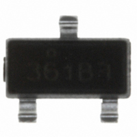
FDN361BN Fairchild Semiconductor, FDN361BN Datasheet - Page 2

FDN361BN
Manufacturer Part Number
FDN361BN
Description
MOSFET N-CH 30V 1.4A SSOT3
Manufacturer
Fairchild Semiconductor
Series
PowerTrench®r
Datasheet
1.FDN361BN.pdf
(5 pages)
Specifications of FDN361BN
Fet Type
MOSFET N-Channel, Metal Oxide
Fet Feature
Logic Level Gate
Rds On (max) @ Id, Vgs
110 mOhm @ 1.4A, 10V
Drain To Source Voltage (vdss)
30V
Current - Continuous Drain (id) @ 25° C
1.4A
Vgs(th) (max) @ Id
3V @ 250µA
Gate Charge (qg) @ Vgs
1.8nC @ 4.5V
Input Capacitance (ciss) @ Vds
193pF @ 15V
Power - Max
460mW
Mounting Type
Surface Mount
Package / Case
3-SSOT, SuperSOT-3
Configuration
Single
Transistor Polarity
N-Channel
Resistance Drain-source Rds (on)
0.11 Ohm @ 10 V
Drain-source Breakdown Voltage
30 V
Gate-source Breakdown Voltage
+/- 20 V
Continuous Drain Current
1.4 A
Power Dissipation
500 mW
Maximum Operating Temperature
+ 150 C
Mounting Style
SMD/SMT
Minimum Operating Temperature
- 55 C
Lead Free Status / RoHS Status
Lead free / RoHS Compliant
Other names
FDN361BNTR
Available stocks
Company
Part Number
Manufacturer
Quantity
Price
Part Number:
FDN361BN
Manufacturer:
FAIRCHILD/ن»™ç«¥
Quantity:
20 000
Notes:
1.
Scale 1 : 1 on letter size paper
2.
FDN361BN Rev A1(W)
Electrical Characteristics
Symbol
Off Characteristics
BV
'BV
I
I
On Characteristics
V
R
I
g
Dynamic Characteristics
C
C
C
R
Switching Characteristics
t
t
t
t
Q
Q
Q
Drain–Source Diode Characteristics
V
t
Q
DSS
GSS
D(on)
d(on)
r
d(off)
f
rr
FS
GS(th)
SD
'T
DS(on)
iss
oss
rss
G
g
gs
gd
rr
R
the drain pins. R
Pulse Test: Pulse Width d 300 Ps, Duty Cycle d 2.0%
DSS
TJA
DSS
J
is the sum of the junction-to-case and case-to-ambient thermal resistance where the case thermal reference is defined as the solder mounting surface of
Drain–Source Breakdown Voltage
Breakdown Voltage Temperature
Coefficient
Zero Gate Voltage Drain Current
Gate–Body Leakage
Gate Threshold Voltage
Static Drain–Source
On–Resistance
On–State Drain Current
Forward Transconductance
Input Capacitance
Output Capacitance
Reverse Transfer Capacitance
Gate Resistance
Turn–On Delay Time
Turn–On Rise Time
Turn–Off Delay Time
Turn–Off Fall Time
Total Gate Charge
Gate–Source Charge
Gate–Drain Charge
Drain–Source Diode Forward
Voltage
Diode Reverse Recovery Time
Diode Reverse Recovery Charge
TJC
is guaranteed by design while R
a) 250qC/W when mounted on a
0.02 in
Parameter
2
pad of 2 oz. copper.
(Note 2)
(Note 2)
TCA
is determined by the user's board design.
T
V
I
V
V
V
V
V
V
V
V
V
V
f = 1.0 MHz
V
V
V
V
V
V
I
A
D
F
= 25°C unless otherwise noted
GS
DS
DS
GS
DS
GS
GS
GS
GS
DS
DS
GS
DD
GS
DS
GS
GS
= 1.4 A,
= 250 PA,Referenced to 25qC
= 10 V, I
= 0 V,
= 24 V,
= 24 V, V
= r20 V,
= V
= 10 V,
= 4.5 V,
= 4.5 V,
= 5 V,
= 15 V,
= 15 mV,
= 15 V,
= 10 V,
= 15 V,
= 4.5 V
= 0 V,
Test Conditions
GS
,
D
I
b) 270°C/W when mounted on a
GS
S
= 1.4 A, T
d
= 0.42 A
iF
minimum pad.
= 0 V, T
/d
I
V
V
I
I
I
V
I
V
f = 1.0 MHz
I
R
I
D
D
D
D
D
D
D
GS
DS
DS
GEN
t
GS
= 250 PA
= 250 PA
= 1.4 A
= 1.2 A
= 1.4 A
= 1 A,
= 1.4 A,
= 100 A/µs
= 0 V
= 5 V
= 0 V
= 0 V,
= 6 :
J
J
= 125qC
= 55qC
(Note 2)
Min
3.5
30
1
Typ Max Units
120
114
145
2.1
1.6
1.3
0.5
0.5
0.8
26
92
35
15
16
11
4
3
8
2
4
r100
110
160
150
193
www.fairchildsemi.com
1.8
1.2
10
47
23
16
29
22
1
3
6
4
mV/qC
m:
nC
nC
nC
nC
PA
PA
nA
pF
pF
pF
nS
ns
ns
ns
ns
:
V
V
A
S
V


