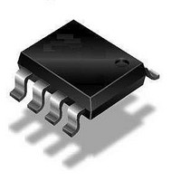
U4083B-MFPG3Y Atmel, U4083B-MFPG3Y Datasheet - Page 4

U4083B-MFPG3Y
Manufacturer Part Number
U4083B-MFPG3Y
Description
Audio Amplifiers COM.CORDED AUDIO AMP
Manufacturer
Atmel
Datasheet
1.U4083B-MFPY_19.pdf
(16 pages)
Specifications of U4083B-MFPG3Y
Product
Class-AB
Output Power
400 mW
Available Set Gain
80 dB
Thd Plus Noise
0.6 %, 0.5 %
Operating Supply Voltage
3 V, 5 V, 9 V
Supply Current
0.065 mA
Maximum Power Dissipation
440 mW
Maximum Operating Temperature
+ 70 C
Mounting Style
SMD/SMT
Audio Load Resistance
100 Ohms
Input Bias Current (max)
0.2 uA
Input Signal Type
Single
Minimum Operating Temperature
- 20 C
Output Signal Type
Differential
Supply Type
Single
Supply Voltage (max)
16 V
Supply Voltage (min)
2 V
Output Type
1-Channel Mono
Package / Case
SOIC-8
Available stocks
Company
Part Number
Manufacturer
Quantity
Price
Part Number:
U4083B-MFPG3Y
Manufacturer:
ATMEL/爱特梅尔
Quantity:
20 000
Part Number:
U4083B-MFPG3Y 19
Manufacturer:
ATMEL/爱特梅尔
Quantity:
20 000
3.3
3.4
4
Pin 4: Amplifier Input V
Pin 6: Supply and Power Dissipation
U4083B
There are two identical operational amplifiers. Amplifier 1 has an open-loop gain
100Hz
R
approximately 1.5 MHz. A closed-loop gain of 46 dB is recommended for a frequency range of
300Hz to 3400Hz (voice band). Amplifier 2 is internally set to a gain of –1.0 dB (0 dB). The out-
puts of both amplifiers are capable of sourcing and sinking a peak current of 200 mA. Output
voltage swing is between 0.4V and V
Figure 8-19 on page
The output DC offset voltage between Pins 5 and 8 (V
back resistor, R
Bias current of Amplifier 1 which is constant with respect to V
through R
amount.
The output offset voltage specified in the electrical characteristics is measured with the feedback
resistor (R
account the bias current as well as internal offset voltages of the amplifiers.
Power dissipation is shown in
Distortion characteristics are given in
where
T
T
R
Power dissipated within the IC in a given application is found from the following equation:
P
I
I
The IC's operating range is defined by a peak operating load current of ±200 mA
page 9
ure 8-14 on page
power level at which 10% distortion occurs. The center flat portion of each curve is defined by
the maximum output current capability of the integrated circuit. The right (descending) portion of
each curve is defined by the maximum internal power dissipation of the IC at 25°C. At higher
ambient temperatures, the maximum load power must be reduced according to the above men-
tioned equation.
P
S
RMS
jmax
amb
tot
i
thJA
totmax
is obtained from
(Figure 8-3 on page
= (V
is the RMS current at the load R
= Ambient temperature
= Junction temperature = 140°C
= Thermal resistance, junction-ambient
(Figure 8-2 on page
to
S
=
f
Figure 8-13 on page
, forcing V
f
T
-------------------------------- -
= 75 k ) shown in the typical application circuit,
i
, Pin 5: Amplifier Output 1 V
I
jmax
S
) + (I
R
f
, because the input offset voltages of the two amplifiers neutralize each other.
thJA
–
12). The left (ascending) portion of each of the three curves is defined by the
T
RMS
Figure 8-15 on page
amb
O1
13).
to shift negative by an amount equal to R
8). The amplifier is unity gain stable, and has a unity gain frequency of
V
S
) – (R
7), whereas the closed-loop gain is set by external resistors, R
Figure 8-8 on page 9
11). It is further specified with respect to different loads (see
L
L
I
S
Figure 8-11 on page 10
RMS
.
– 1.3V at maximum current
12.
2
)
O1
, Pin 8: Amplifier Output 2 V
to
Figure 8-10 on page 10
O1
– V
Figure 8-20 on page
O2
to
) is mainly a function of the feed-
Figure 8-13 on page
f
I
IB
s
, flows out of Pin 4 (V
(Figure 8-18 on page 13
and V
O2
positive to an equal
for different loads.
14. It takes into
4655C–CORD–03/06
(Figure 8-8 on
11.
O2
80 dB at
i
) and
f
Fig-
and
and


