SI4396DY-T1-E3 Vishay, SI4396DY-T1-E3 Datasheet
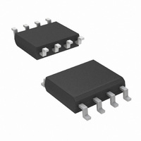
MOSFET N-CH 30V 16A 8-SOIC

SI4396DY-T1-E3

Manufacturer Part Number
SI4396DY-T1-E3
Description
MOSFET N-CH 30V 16A 8-SOIC
Manufacturer
Vishay
Series
TrenchFET®r
Datasheet

Specifications of SI4396DY-T1-E3

Fet Type
MOSFET N-Channel, Metal Oxide
Fet Feature
Standard
Rds On (max) @ Id, Vgs
11.5 mOhm @ 10A, 10V
Drain To Source Voltage (vdss)
30V
Current - Continuous Drain (id) @ 25° C
16A
Vgs(th) (max) @ Id
2.6V @ 250µA
Gate Charge (qg) @ Vgs
45nC @ 10V
Input Capacitance (ciss) @ Vds
1675pF @ 15V
Power - Max
5.4W
Mounting Type
Surface Mount
Package / Case
8-SOIC (3.9mm Width)
Transistor Polarity
N Channel + Schottky Diode
Continuous Drain Current Id
16A
Drain Source Voltage Vds
30V
On Resistance Rds(on)
16mohm
Rds(on) Test Voltage Vgs
20V
Configuration
Single Quad Drain Triple Source
Resistance Drain-source Rds (on)
0.0115 Ohms
Drain-source Breakdown Voltage
30 V
Gate-source Breakdown Voltage
+/- 20 V
Continuous Drain Current
12.3 A
Power Dissipation
3.1 W
Maximum Operating Temperature
+ 150 C
Mounting Style
SMD/SMT
Minimum Operating Temperature
- 55 C
Lead Free Status / RoHS Status
Lead free / RoHS Compliant
Lead Free Status / RoHS Status
Lead free / RoHS Compliant, Lead free / RoHS Compliant
Other names
SI4396DY-T1-E3TR

Available stocks

Company
Part Number
Manufacturer
Quantity
Price
Part Number:
SI4396DY-T1-E3
Manufacturer:
TI
Quantity:
1 785
Part Number:
SI4396DY-T1-E3
Manufacturer:
VISHAY/威世
Quantity:
20 000
Notes:
a. Based on T
b. Surface Mounted on 1" x 1" FR4 board.
c. t = 10 s.
d. Maximum under Steady State conditions is 85 °C/W.
Document Number: 74252
S09-0392-Rev. B, 09-Mar-09
Ordering Information:
ABSOLUTE MAXIMUM RATINGS T
Parameter
Drain-Source Voltage
Gate-Source Voltage
Continuous Drain Current (T
Pulsed Drain Current
Continuous Source-Drain Diode Current
Single Pulse Avalanche Current
Single Pulse Avalanche Energy
Maximum Power Dissipation
Operating Junction and Storage Temperature Range
THERMAL RESISTANCE RATINGS
Parameter
Maximum Junction-to-Ambient
Maximum Junction-to-Foot (Drain)
PRODUCT SUMMARY
SCHOTTKY AND BODY DIODE PRODUCT
SUMMARY
V
V
DS
DS
30
30
(V)
(V)
G
S
S
S
C
= 25 °C.
1
2
3
4
N-Channel 30-V (D-S) MOSFET with Schottky Diode
0.0115 at V
0.016 at V
Diode Forward Voltage
R
Si4396DY-T1-E3
Si4396DY
Top V ie w
DS(on)
SO-8
GS
0.4 at 2 A
GS
V
(Ω)
J
= 4.5 V
-T1-GE3 (Lead (Pb)-free and Halogen-free)
SD
= 10 V
= 150 °C)
b, d
(V)
8
7
6
5
(Lead (Pb)-free)
D
D
D
D
I
D
12.7
16
(A)
a
A
= 25 °C, unless otherwise noted
Q
Steady State
13.3 nC
I
g
S
5
(Typ.)
t ≤ 10 s
(A)
a
T
T
T
T
T
T
L = 0.1 mH
T
T
T
T
C
C
C
C
C
A
A
A
A
A
= 25 °C
= 70 °C
= 25 °C
= 70 °C
= 25 °C
= 25 °C
= 25 °C
= 70 °C
= 25 °C
= 70 °C
FEATURES
APPLICATIONS
Halogen-free According to IEC 61249-2-21
Available
TrenchFET
100 % R
Notebook Logic DC/DC
- Low Side
Symbol
R
R
thJA
thJF
Symbol
T
N-Channel MOSFET
J
V
g
V
E
I
I
P
, T
DM
I
I
AS
DS
GS
AS
D
S
and UIS Tested
D
®
stg
Power MOSFET
G
Typ.
34
17
- 55 to 150
D
S
12.3
9.7
2.8
3.1
2.0
Limit
± 20
12.7
5.4
3.4
30
16
40
20
20
5
b, c
b, c
b, c
b, c
b, c
Vishay Siliconix
Schottky Diode
Max.
40
23
Si4396DY
www.vishay.com
Unit
mJ
°C
W
V
A
°C/W
Unit
1

Related parts for SI4396DY-T1-E3

SI4396DY-T1-E3 Summary of contents

Page 1

... Top Ordering Information: Si4396DY-T1-E3 (Lead (Pb)-free) Si4396DY -T1-GE3 (Lead (Pb)-free and Halogen-free) ABSOLUTE MAXIMUM RATINGS T Parameter Drain-Source Voltage Gate-Source Voltage Continuous Drain Current (T = 150 °C) J Pulsed Drain Current Continuous Source-Drain Diode Current Single Pulse Avalanche Current Single Pulse Avalanche Energy Maximum Power Dissipation ...

Page 2

... Si4396DY Vishay Siliconix SPECIFICATIONS °C, unless otherwise noted J Parameter Static Drain-Source Breakdown Voltage Gate-Source Threshold Voltage Gate-Source Leakage Zero Gate Voltage Drain Current a On -State Drain Current a Drain-Source On-State Resistance a Forward Transconductance b Dynamic Input Capacitance Output Capacitance Reverse Transfer Capacitance Total Gate Charge ...

Page 3

... Q - Total Gate Charge (nC) g Gate Charge Document Number: 74252 S09-0392-Rev. B, 09-Mar- thru 1.5 2.0 2 18.6 24.8 31.0 Si4396DY Vishay Siliconix 2.0 1.6 1 125 ° °C C 0 Gate-to-Source Voltage (V) GS Transfer Characteristics 2200 1760 C iss 1320 880 C oss ...

Page 4

... Si4396DY Vishay Siliconix TYPICAL CHARACTERISTICS 25 °C, unless otherwise noted 100 T = 150 ° ° 0.1 0.0 0.2 0 Source-to-Drain Voltage (V) SD Source-Drain Diode Forward Voltage Junction Temperature (°C) J Reverse Current (Schottky) www.vishay.com 4 0.6 1 0.8 100 125 150 100 Limited DS(on 0 °C A Single Pulse ...

Page 5

... T - Case Temperature (°C) C Current Derating* 100 125 150 = 150 °C, using junction-to-case thermal resistance, and is more useful in settling the upper J(max) Si4396DY Vishay Siliconix 125 150 2.0 1.6 1.2 0.8 0.4 0 100 T - Ambient Temperature (°C) A Power Derating, Junction-to-Ambient www.vishay.com 125 ...

Page 6

... Si4396DY Vishay Siliconix TYPICAL CHARACTERISTICS 25 °C, unless otherwise noted 1 Duty Cycle = 0.5 0.2 0.1 0.1 0.05 0.02 Single Pulse 0. Duty Cycle = 0.5 0.2 0.1 0.1 0.05 0.02 Single Pulse 0. Vishay Siliconix maintains worldwide manufacturing capability. Products may be manufactured at one of several qualified locations. Reliability data for Silicon Technology and Package Reliability represent a composite of all qualified locations ...

Page 7

... Vishay disclaims any and all liability arising out of the use or application of any product described herein or of any information provided herein to the maximum extent permitted by law. The product specifications do not expand or otherwise modify Vishay’ ...

Related keywords