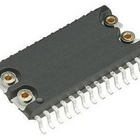
M41T11MH6 STMicroelectronics, M41T11MH6 Datasheet - Page 9

M41T11MH6
Manufacturer Part Number
M41T11MH6
Description
Real Time Clock Serial 512 (64x8)
Manufacturer
STMicroelectronics
Datasheet
1.M41T11MH6.pdf
(30 pages)
Specifications of M41T11MH6
Function
Clock, Calendar, Timekeeper
Rtc Memory Size
64 B
Supply Voltage (max)
5.5 V
Supply Voltage (min)
2 V
Maximum Operating Temperature
+ 85 C
Minimum Operating Temperature
- 40 C
Mounting Style
SMD/SMT
Rtc Bus Interface
Serial
Package / Case
SO-28
Time Format
HH:MM:SS
Lead Free Status / RoHS Status
Lead free / RoHS Compliant
Available stocks
Company
Part Number
Manufacturer
Quantity
Price
Company:
Part Number:
M41T11MH6E
Manufacturer:
ST
Quantity:
465
Part Number:
M41T11MH6E
Manufacturer:
ST
Quantity:
20 000
Company:
Part Number:
M41T11MH6F
Manufacturer:
ST
Quantity:
1 000
Part Number:
M41T11MH6F
Manufacturer:
ST
Quantity:
20 000
M41T11
2.1.3
2.1.4
2.1.5
Figure 5.
CLOCK
DATA
Stop data transfer
A change in the state of the data line, from low to high, while the clock is high, defines the
STOP condition.
Data valid
The state of the data line represents valid data when after a start condition, the data line is
stable for the duration of the high period of the clock signal. The data on the line may be
changed during the low period of the clock signal. There is one clock pulse per bit of data.
Each data transfer is initiated with a start condition and terminated with a stop condition.
The number of data bytes transferred between the start and stop conditions is not limited.
The information is transmitted byte-wide and each receiver acknowledges with a ninth bit.
By definition, a device that gives out a message is called “transmitter”, the receiving device
that gets the message is called “receiver”. The device that controls the message is called
“master”. The devices that are controlled by the master are called “slaves”.
Acknowledge
Each byte of eight bits is followed by one acknowledge bit. This acknowledge bit is a low
level put on the bus by the receiver, whereas the master generates an extra acknowledge
related clock pulse.
A slave receiver which is addressed is obliged to generate an acknowledge after the
reception of each byte. Also, a master receiver must generate an acknowledge after the
reception of each byte that has been clocked out of the slave transmitter.
The device that acknowledges has to pull down the SDA line during the acknowledge clock
pulse in such a way that the SDA line is a stable low during the high period of the
acknowledge related clock pulse. Of course, setup and hold times must be taken into
account. A master receiver must signal an end-of-data to the slave transmitter by not
generating an acknowledge on the last byte that has been clocked out of the slave. In this
case, the transmitter must leave the data line high to enable the master to generate the
STOP condition.
Serial bus data transfer sequence
CONDITION
START
DATA VALID
DATA LINE
STABLE
DATA ALLOWED
CHANGE OF
CONDITION
STOP
AI00587
Operation
9/30


