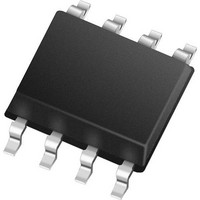
MCP79412-I/ST Microchip Technology, MCP79412-I/ST Datasheet - Page 20

MCP79412-I/ST
Manufacturer Part Number
MCP79412-I/ST
Description
Real Time Clock I2C GP RTCC 1Kb EE 64B SRAM EUI-64
Manufacturer
Microchip Technology
Series
-r
Type
Clock/Calendarr
Datasheet
1.MCP79412-ISN.pdf
(40 pages)
Specifications of MCP79412-I/ST
Function
Clock/Calendar
Rtc Memory Size
64 Byte
Maximum Operating Temperature
+ 85 C
Minimum Operating Temperature
- 40 C
Rtc Bus Interface
I2C
Supply Current
1 uA
Features
Alarm, Leap Year, NVSRAM, Square Wave Output, Unique ID
Memory Size
64B
Time Format
HH:MM:SS (12/24 hr)
Date Format
YY-MM-DD-dd
Interface
I²C
Voltage - Supply
1.8 V ~ 5.5 V
Voltage - Supply, Battery
1.3 V ~ 5.5 V
Operating Temperature
-40°C ~ 85°C
Mounting Type
Surface Mount
Package / Case
8-TSSOP (0.173", 4.40mm Width)
Lead Free Status / RoHS Status
Lead free / RoHS Compliant
MCP7941X
FIGURE 5-3:
FIGURE 5-4:
5.2.3
The EEPROM does not support a hardware write
protection pin, however, software block protection is
available to the use and is configured using the
STATUS register. Please refer to Section
“STATUS REGISTER”
5.2.4
Read operations are initiated in the same way as write
operations with the exception that the R/W bit of the
control byte is set to one. There are three basic types
of read operations: current address read, random read,
and sequential read.
5.2.4.1
The MCP7941X contains an address counter that
maintains the address of the last word accessed,
internally incremented by one. Therefore, if the
previous read access was to address n (n is any legal
address), the next current address read operation
would access data from address n + 1. In the case of a
page write, if the last byte written is the last byte of a
page, the next address location would be the first byte
of the same page written.
Upon receipt of the control byte with R/W bit set to one,
the MCP7941X issues an Acknowledge and transmits
the 8-bit data word. The master will not acknowledge
the transfer but does generate a Stop condition and the
MCP7941X discontinues transmission
DS22266C-page 20
BUS ACTIVITY
MASTER
SDA LINE
BUS ACTIVITY
Current Address Read
BLOCK PROTECTION
READ OPERATION
EE BYTE WRITE
EE PAGE WRITE
BUS ACTIVITY
MASTER
SDA LINE
BUS ACTIVITY
for more details.
S
T
A
R
T
S 1 0 1 0
CONTROL
BYTE
1 1 1
(Figure
S 1 0 1 0
S
T
A
R
T
0
A
C
K
CONTROL
5-1).
0
BYTE
4.2.1
ADDRESS
1 1 1
BYTE
0
A
C
K
0
ADDRESS
A
C
K
FIGURE 5-1:
5.2.4.2
Random read operations allow the master to access
any memory location in a random manner. To perform
this type of read operation, first the word address must
be set. This is done by sending the word address to the
MCP7941X as part of a write operation (R/W bit set to
‘0’). After the word address is sent, the master
generates a Start condition following the Acknowledge.
This terminates the write operation, but not before the
internal Address Pointer is set. Then, the master issues
the control byte again but with the R/W bit set to a one.
The MCP7941X will then issue an Acknowledge and
transmit the 8-bit data word. The master will not
acknowledge the transfer but it does generate a Stop
condition which causes the MCP7941X to discontinue
transmission
command, the internal address counter will point to the
address location following the one that was just read.
BUS ACTIVITY
MASTER
SDA LINE
BUS ACTIVITY
BYTE
DATA BYTE 0
Random Read
A
C
K
S
S
T
A
R
T
(Figure
1
A
C
K
CURRENT ADDRESS READ
(EEPROM SHOWN)
0
2010-2011 Microchip Technology Inc.
CONTROL
DATA
1
BYTE
0
5-2). After a random read
DATA BYTE 7
1 1 1
1
A
C
K
A
C
K
S
T
O
P
P
A
C
K
DATA
BYTE
S
T
O
P
P
O
N
A
C
K
S
T
O
P
P


