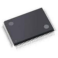
ISPPAC-CLK5510V-01T48I Lattice, ISPPAC-CLK5510V-01T48I Datasheet - Page 34

ISPPAC-CLK5510V-01T48I
Manufacturer Part Number
ISPPAC-CLK5510V-01T48I
Description
Clock Drivers & Distribution PROGRAMMABLE CLOCK GENERATOR
Manufacturer
Lattice
Datasheet
1.PAC-SYSTEMCLK5520.pdf
(48 pages)
Specifications of ISPPAC-CLK5510V-01T48I
Minimum Operating Temperature
- 40 C
Mounting Style
SMD/SMT
Maximum Operating Temperature
85 C
Package / Case
TQFP-100
Lead Free Status / RoHS Status
Lead free / RoHS Compliant
Available stocks
Company
Part Number
Manufacturer
Quantity
Price
Company:
Part Number:
ISPPAC-CLK5510V-01T48I
Manufacturer:
Lattice Semiconductor Corporation
Quantity:
10 000
Lattice Semiconductor
Figure 30. PAC-Designer Design Entry Screen (ispClock5520)
In-System Programming
The ispClock5500 is an In-System Programmable (ISP™) device. This is accomplished by integrating all E
configuration control logic on-chip. Programming is performed through a 4-wire, IEEE 1149.1 compliant serial JTAG
interface at normal logic levels. Once a device is programmed, all configuration information is stored on-chip, in
non-volatile E
tions are described in the JTAG interface section of this data sheet.
User Electronic Signature
A user electronic signature (UES) feature is included in the E
32 bits that can be configured by the user to store unique data such as ID codes, revision numbers or inventory
control data. The specifics this feature are discussed in the IEEE 1149.1 serial interface section of this data sheet.
Electronic Security
An electronic security “fuse” (ESF) bit is provided in every ispClock5500 device to prevent unauthorized readout of
the E
bits in the device. This cell can only be erased by reprogramming the device, so the original configuration can not
be examined once programmed. Usage of this feature is optional. The specifics of this feature are discussed in the
IEEE 1149.1 serial interface section of this data sheet.
Production Programming Support
Once a final configuration is determined, an ASCII format JEDEC file can be created using the PAC-Designer soft-
ware. Devices can then be ordered through the usual supply channels with the user’s specific configuration already
preloaded into the devices. By virtue of its standard interface, compatibility is maintained with existing production
programming equipment, giving customers a wide degree of freedom and flexibility in production planning.
Evaluation Fixture
Included in the basic ispClock5500 Design Kit is an engineering prototype board that can be connected to the par-
allel port of a PC using a Lattice ispDOWNLOAD
ispClock5500 and can be used in real time to check circuit operation as part of the design process. Input and out-
put connections (SMA connectors for all RF signals) are provided to aid in the evaluation of the ispClock5500 for a
given application. (Figure 31).
PAC-SYSTEMCLK5520
PACCLK5520-EV
2
CMOS configuration bit patterns. Once programmed, this cell prevents further access to the functional user
2
CMOS memory cells. The specifics of the IEEE 1149.1 serial interface and all ispClock5500 instruc-
Part Number
Complete system kit, evaluation board, ispDOWNLOAD cable and software.
Evaluation board only, with components, fully assembled.
®
cable. It demonstrates proper layout techniques for the
34
2
CMOS memory of the ispClock5500. This consists of
Description
ispClock5500 Family Data Sheet
2
CMOS


