NB100LVEP224FA ON Semiconductor, NB100LVEP224FA Datasheet

Clock Drivers & Distribution 2.5V/3.3V 1:24 Diff

NB100LVEP224FA

Manufacturer Part Number
NB100LVEP224FA
Description
Clock Drivers & Distribution 2.5V/3.3V 1:24 Diff
Manufacturer
ON Semiconductor
Type
ECL, LVDS, PECLr
Datasheet

Specifications of NB100LVEP224FA

Max Output Freq
1 GHz
Minimum Operating Temperature
- 40 C
Mounting Style
SMD/SMT
Multiply / Divide Factor
2:1
Number Of Clock Inputs
2
Output Logic Level
ECL
Supply Voltage (max)
+/- 3.8 V
Supply Voltage (min)
+/- 2.375 V
Maximum Operating Temperature
+ 85 C
Package / Case
LQFP-64 Exposed Pad
Lead Free Status / RoHS Status
Lead free / RoHS Compliant

Available stocks

Company
Part Number
Manufacturer
Quantity
Price
Part Number:
NB100LVEP224FAG
Manufacturer:
ON Semiconductor
Quantity:
135
Part Number:
NB100LVEP224FAG
Manufacturer:
ON Semiconductor
Quantity:
15
Part Number:
NB100LVEP224FAG
Manufacturer:
ON Semiconductor
Quantity:
10 000
Part Number:
NB100LVEP224FAR2
Manufacturer:
ON Semiconductor
Quantity:
10 000
Part Number:
NB100LVEP224FARG
Manufacturer:
ON Semiconductor
Quantity:
10 000
NB100LVEP224
2.5V/3.3V 1:24 Differential
ECL/PECL Clock Driver with
Clock Select and Output
Enable
Description
driver, designed with clock distribution in mind, accepting two clock
sources into an input multiplexer. The part is designed for use in low
voltage applications which require a large number of outputs to drive
precisely aligned low skew signals to their destination. The two clock
inputs are differential ECL/PECL and they are selected by the
CLK_SEL pin. To avoid generation of a runt clock pulse when the
device is enabled/disabled, the Output Enable (OE) is synchronous
ensuring the outputs will only be enabled/disabled when they are
already in LOW state (See Figure 4).
optimal design, layout, and processing minimize skew within a device
and from lot to lot. In any differential output, the same bias and
termination scheme is required. Unused output pairs should be left
unterminated (open) to “reduce power and switching noise as much as
possible.” Any unused single line of a differential pair should be
terminated the same as the used line to maintain balanced loads on the
differential driver outputs. The wide VIHCMR specification allows
both pair of CLOCK inputs to accept LVDS levels.
operated from a positive V
the LVEP224 to be used for high performance clock distribution in
+3.3 V or +2.5 V systems. Single-ended CLK input operation is
limited to a V
mode. In a PECL environment, series or Thevenin line terminations
are typically used as they require no additional power supplies. For
more information on PECL terminations, designers should refer to
Application Note AND8020/D.
Features
*For additional information on our Pb-Free strategy and soldering details, please
© Semiconductor Components Industries, LLC, 2008
March, 2008 - Rev. 8
download the ON Semiconductor Soldering and Mounting Techniques
Reference Manual, SOLDERRM/D.
The NB100LVEP224 is a low skew 1-to-24 differential clock
The NB100LVEP224 guarantees low output-to-output skew. The
The NB100LVEP224, as with most other ECL devices, can be
20 ps Typical Output-to-Output Skew
75 ps Typical Device-to-Device Skew
Maximum Frequency > 1 GHz
650 ps Typical Propagation Delay
LVPECL Mode Operating Range:
V
NECL Mode Operating Range:
V
CC
CC
= 2.375 V to 3.8 V with V
= 0 V with V
CC
≥ 3.0 V in LVPECL mode, or V
EE
= -2.375 V to -3.8 V
CC
supply in LVPECL mode. This allows
EE
= 0 V
EE
≤ -3.0 V in NECL
1
Internal Input Pulldown Resistors
Q Output will Default Low with Inputs Open or at V
Thermally Enhanced 64-Lead LQFP
CLOCK Inputs are LVDS-Compatible; Requires
External 100 W LVDS Termination Resistor
Pb-Free Packages are Available*
*For additional marking information, refer to
See detailed ordering and shipping information in the package
dimensions section on page 8 of this data sheet.
Application Note AND8002/D.
CASE 848G
FA SUFFIX
LQFP-64
A
WL
YY
WW
G
ORDERING INFORMATION
http://onsemi.com
= Assembly Location
= Wafer Lot
= Year
= Work Week
= Pb-Free Package
Publication Order Number:
64
DIAGRAM*
1
MARKING
AWLYYWWG
NB100LVEP224/D
LVEP224
NB100
EE

Related parts for NB100LVEP224FA

NB100LVEP224FA Summary of contents

Page 1

... NECL Mode Operating Range with V = -2.375 *For additional information on our Pb-Free strategy and soldering details, please download the ON Semiconductor Soldering and Mounting Techniques Reference Manual, SOLDERRM/D. © Semiconductor Components Industries, LLC, 2008 March, 2008 - Rev. 8 ≤ -3 NECL EE • Internal Input Pulldown Resistors • ...

Page 2

V 49 CCO CCO 1 2 ...

Page 3

Table 3. ATTRIBUTES Internal Input Pulldown Resistor Internal Input Pullup Resistor ESD Protection Moisture Sensitivity, Indefinite Time Out of Drypack (Note 2) Flammability Rating Transistor Count Meets or exceeds JEDEC Spec EIA/JESD78 IC Latchup Test 2. ...

Page 4

Table 5. LVPECL DC CHARACTERISTICS Symbol Characteristic I Power Supply Current EE V Output HIGH Voltage (Note Output LOW Voltage (Note Input HIGH Voltage (Single-Ended) IH (Note 5) V Input LOW Voltage (Single-Ended) IL ...

Page 5

Table 7. NECL DC CHARACTERISTICS Symbol Characteristic I Power Supply Current Output HIGH Voltage (Note 12 Output LOW Voltage (Note 12 Input HIGH Voltage (Single-Ended) IH (Note 13) V Input ...

Page 6

V 500 3.3 V 400 300 200 0.5 0.6 0.7 INPUT FREQUENCY (GHz) Figure 3. Output Amplitude (V ) versus Input Frequency and Random Clock Jitter (t OPP CLK CLK Figure 4. ...

Page 7

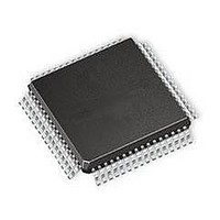
Using the thermally enhanced package of the NB100LVEP224 The NB100LVEP224 uses a thermally enhanced 64-lead LQFP package. The package is molded so that a portion of the leadframe is exposed at the surface of the package bottom side. This exposed ...

Page 8

... ORDERING INFORMATION Device NB100LVEP224FA NB100LVEP224FAG NB100LVEP224FAR2 NB100LVEP224FARG †For information on tape and reel specifications, including part orientation and tape sizes, please refer to our Tape and Reel Packaging Specifications Brochure, BRD8011/D. Resource Reference of Application Notes AN1405/D AN1406/D AN1503/D AN1504/D AN1568/D AN1672/D AND8001/D - Odd Number Counters Design ...

Page 9

M M - A/2 A DETAIL AH -T- AG G/2 SEATING 4 PL PLANE 0.08 (0.003 EXPOSED PAD ...

Page 10

... Opportunity/Affirmative Action Employer. This literature is subject to all applicable copyright laws and is not for resale in any manner. PUBLICATION ORDERING INFORMATION LITERATURE FULFILLMENT:  Literature Distribution Center for ON Semiconductor  P.O. Box 5163, Denver, Colorado 80217 USA  Phone: 303-675-2175 or 800-344-3860 Toll Free USA/Canada  Fax: 303-675-2176 or 800-344-3867 Toll Free USA/Canada   ...

Related keywords