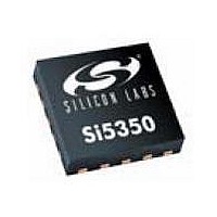
Si5350A-A-GM Silicon Laboratories Inc, Si5350A-A-GM Datasheet - Page 11

Si5350A-A-GM
Manufacturer Part Number
Si5350A-A-GM
Description
Clock Generators & Support Products Any-Rate Dual PLL 125MHz Clk 8 outputs
Manufacturer
Silicon Laboratories Inc
Type
Any Frequency CMOS Clock Generatorr
Datasheet
1.SI5350A-A-GM.pdf
(20 pages)
Specifications of Si5350A-A-GM
Mounting Style
SMD/SMT
Max Input Freq
0.008 MHz
Max Output Freq
125 MHz
Number Of Outputs
8
Operating Supply Voltage
3.3 V
Operating Temperature Range
- 40 C to + 85 C
Supply Current
25 mA
Package / Case
QFN-20
Lead Free Status / RoHS Status
Lead free / RoHS Compliant
Up to two frequency select pins are available on the Si5350A. Each of the frequency select pins can be linked to
any of the clock outputs as shown in Figure 6. For example, FS_0 can be linked to control clock frequency
selection on CLK0, CLK3, and CLK5; FS_1 can be used to control clock frequency selection on CLK1, CLK2, and
CLK4. Any other combination is also possible.
The Si5350A uses control circuitry to ensure that frequency changes are glitchless. This ensures that the clock
always completes its last cycle before starting a new clock cycle of a different frequency.
4.3.4. Output Enable (OEB_0, OEB_1, OEB_2)
Up to three output enable pins (OEB_0/1/2) are available on the Si5350A. Similar to the FS pins, each OEB pin can
be linked to any of the output clocks. In the example shown in Figure 7, OEB_0 is linked to control CLK0, CLK3,
and CLK5; OEB_1 is linked to control CLK6 and CLK7, and OEB_2 is linked to control CLK1, CLK2, CLK4, and
CLK5. Any other combination is also possible. If more than one OEB pin is linked to the same CLK output, the pin
forcing a disable state will be dominant. Clock outputs are enabled when the OEB pin is held low.
The output enable control circuitry ensures glitchless operation by starting the output clock cycle on the first leading
edge after OEB is asserted (OEB = low). When OEB is released (OEB = high), the clock is allowed to complete its
full clock cycle before going into a disabled state. This is shown in Figure 7. When disabled, the output state is
configurable as disabled high, disabled low, or disabled in high-impedance.
FS_1
FS_0
0
1
0
1
OEB_0
OEB_1
OEB_2
F1_1, F1_2, F1_4
F2_1, F2_2, F2_4
Output Frequency
F1_0, F1_3, F1_5
F2_0, F2_3, F2_5
Output Frequency
0
1
0
1
0
1
CLK Disabled
CLK Disabled
CLK Disabled
CLK Enabled
Output State
Output State
CLK Enabled
Output State
CLK Enabled
Figure 6. Example Configuration of a Pin-Controlled Frequency Select (FS)
Figure 7. Example Configuration of a Pin-Controlled Output Enable
FS_0
FS_1
OEB_0
OEB_1
OEB_2
Customizable FS Control
Customizable OEB Control
Cannot be controlled
by FS pins
FS
FS
FS
FS
FS
FS
MultiSynth 0
MultiSynth 1
MultiSynth 5
MultiSynth 2
MultiSynth 3
MultiSynth 4
OEB
OEB
OEB
OEB
OEB
OEB
OEB
OEB
Rev. 0.2
CLK0
CLK1
CLK2
CLK3
CLK4
CLK5
CLK6
CLK7
CLK0
CLK1
CLK2
CLK3
CLK4
CLK5
CLK6
CLK7
CLKx
OEBx
CLKx
Frequency_A
Glitchless Frequency Changes
changing to a new frequency
Full cycle completes before
Clock starts on the
first leading edge
Glitchless Output Enable
New frequency starts
at its leading edge
Frequency_B
Clock continues until
cycle is complete
Si5350A
Frequency_A
11


