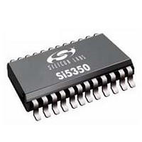
Si5350A-A-GU Silicon Laboratories Inc, Si5350A-A-GU Datasheet - Page 8

Si5350A-A-GU
Manufacturer Part Number
Si5350A-A-GU
Description
Clock Generators & Support Products Any-Rate Dual PLL 125MHz Clk 8 outputs
Manufacturer
Silicon Laboratories Inc
Type
Any Frequency CMOS Clock Generatorr
Datasheet
1.SI5350A-A-GM.pdf
(20 pages)
Specifications of Si5350A-A-GU
Mounting Style
SMD/SMT
Max Input Freq
0.008 MHz
Max Output Freq
125 MHz
Number Of Outputs
8
Operating Supply Voltage
3.3 V
Operating Temperature Range
- 40 C to + 85 C
Supply Current
25 mA
Package / Case
QSOP-24
Lead Free Status / RoHS Status
Lead free / RoHS Compliant
Si5350A
3. Functional Description
The Si5350A’s synthesis architecture consists of two high-frequency PLLs in addition to one high-resolution
fractional MultiSynth
Figure 2. This unique architecture allows the Si5350A to generate up to eight independent, non-integer-related
frequencies at any of its outputs. Each MultiSynth
a pin controlled glitchless frequency change at each output (CLK0 to CLK5).
8
Figure 2. Block Diagrams of 3-Output and 8-Output Si5350A Devices
TM
divider per output. A block diagram of both the 3-output and 8-output versions are shown in
XA
XB
P0
P1
XA
XB
P0
P1
P2
P3
P4
10-MSOP
OSC
OSC
Control
Control
Logic
VDD
GND
Logic
PLL
PLL
PLL
PLL
A
B
A
B
VDD
GND
TM
is configurable with two frequencies (F1_x, F2_x). This allows
Rev. 0.2
FS
FS
FS
FS
FS
FS
FS
FS
FS
20-QFN, 24-QSOP
MultiSynth 6
MultiSynth 0
MultiSynth 1
MultiSynth 2
MultiSynth 3
MultiSynth 0
MultiSynth 1
MultiSynth 2
MultiSynth 3
MultiSynth 4
MultiSynth 5
MultiSynth 7
F1_6
F1_0
F2_0
F1_1
F2_1
F1_2
F2_2
F1_0
F2_0
F1_1
F2_1
F1_2
F2_2
F1_3
F2_3
F1_4
F2_4
F1_5
F2_5
F1_7
R6
R7
R0
R1
R2
R0
R1
R2
R3
R4
R5
VDDO
VDDOC
VDDOD
VDDOB
CLK6
CLK2
VDDOA
CLK2
CLK4
CLK7
CLK0
CLK1
CLK0
CLK1
CLK3
CLK5


