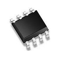
M41T0M6 STMicroelectronics, M41T0M6 Datasheet - Page 13

M41T0M6
Manufacturer Part Number
M41T0M6
Description
Real Time Clock ENV 511-M41T0M6E
Manufacturer
STMicroelectronics
Datasheet
1.M41T0DW6F.pdf
(22 pages)
Specifications of M41T0M6
Function
Clock, Calendar
Rtc Memory Size
8 B
Supply Voltage (max)
5.5 V
Supply Voltage (min)
2 V
Maximum Operating Temperature
+ 85 C
Minimum Operating Temperature
- 40 C
Mounting Style
SMD/SMT
Rtc Bus Interface
Serial
Package / Case
SO-8
Time Format
HH:MM:SS
Lead Free Status / RoHS Status
Lead free / RoHS Compliant
Available stocks
Company
Part Number
Manufacturer
Quantity
Price
Part Number:
M41T0M6E
Manufacturer:
ST
Quantity:
20 000
Part Number:
M41T0M6F
Manufacturer:
ST
Quantity:
20 000
3
Note:
3.1
Note:
3.2
Clock operation
The M41T0 is driven by a quartz controlled oscillator with a nominal frequency of
32.768 kHz. The accuracy of the real-time clock depends on the frequency of the quartz
crystal that is used as the time-base for the RTC. The M41T0 is tested to meet ± 35 ppm
with nominal crystal. The eight-byte clock register (see
set the clock and to read the date and time from the clock, in a binary coded decimal format.
Seconds, minutes, and hours are contained within the first three registers. Bits D6 and D7 of
clock register 2 (hours register) contain the CENTURY ENABLE bit (CEB) and the
CENTURY bit (CB). Setting CEB to a '1' will cause CB to toggle, either from '0' to '1' or from
'1' to '0' at the turn of the century (depending upon its initial state). If CEB is set to a '0', CB
will not toggle. Bits D0 through D2 of register 3 contain the day (day of week). Registers 4, 5
and 6 contain the date (day of month), month and years. The final register is the control
register. Bit D7 of register 0 contains the STOP bit (ST). Setting this bit to a '1' will cause the
oscillator to stop. If the device is expected to spend a significant amount of time on the shelf,
the oscillator may be stopped to reduce current drain. When reset to a '0' the oscillator
restarts within four seconds (typically one second).
The seven clock registers may be read one byte at a time, or in a sequential block. The
control register (address location 7) may be accessed independently. Provision has been
made to assure that a clock update does not occur while any of the seven clock addresses
are being read. If a clock address is being read, an update of the clock registers will be
delayed by 250 ms to allow the READ to be completed before the update occurs. This will
prevent a transition of data during the READ.
This 250 ms delay affects only the clock register update and does not alter the actual clock
time.
Output driver pin
The OUT pin is an output driver that reflects the contents of D7 of the control register. In
other words, when D7 of location 7 is a '0' then the OUT pin will be driven low.
The OUT pin is open drain which requires an external pull-up resistor.
Oscillator stop detection
If the oscillator fail (OF) bit is internally set to a '1,' this indicates that the oscillator has either
stopped, or was stopped for some period of time and can be used to judge the validity of the
clock and date data. This bit will be set to '1' any time the oscillator stops. The following
conditions can cause the OF bit to be set:
●
●
●
●
This bit will remain set to '1' until written to logic '0.'
The oscillator must start and have run for at least 4 seconds before attempting to reset the
OF bit to '0.' This function operates both under normal power and in battery backup.
The first time power is applied (defaults to a '1' on power-up).
The voltage present on V
The ST bit is set to '1.'
External interference or removal of the crystal.
CC
is insufficient to support oscillation.
Table 3 on page
14) is used to both
13/22


