ZXMP6A18KTC Diodes Zetex, ZXMP6A18KTC Datasheet
ZXMP6A18KTC
Specifications of ZXMP6A18KTC
ZXMP6A18KTCTR


Related parts for ZXMP6A18KTC


ZXMP6A18KTC Summary of contents
Page 1
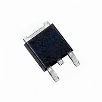
... Low gate drive • DPAK package Applications • Motor drive • Disconnect switches Ordering information Device Reel size (inches) ZXMP6A18KTC 13 Device marking ZXMP 6A18 Issue 1 - March 2006 © Zetex Semiconductors plc 2006 = -10.4A D Tape width Quantity per reel 16mm 2500 units ...
Page 2
Absolute maximum ratings Parameter Drain-source voltage Gate-source voltage Continuous drain current (b) @V =10V; T =25° (b) @V =10V; T =70° (a) @V =10V; T =25° (c) Pulsed drain current Continuous source current (body ...
Page 3
Characteristics Issue 1 - March 2006 © Zetex Semiconductors plc 2006 ZXMP6A18K 3 www.zetex.com ...
Page 4
Electrical characteristics (at T Parameter Static Drain-source breakdown voltage V Zero gate voltage drain current Gate-body leakage Gate-source threshold voltage Static drain-source on-state (*) resistance Forward transconductance (‡) Dynamic Input capacitance Output capacitance Reverse transfer capacitance (†) (‡) Switching Turn-on ...
Page 5
Typical characteristics Issue 1 - March 2006 © Zetex Semiconductors plc 2006 ZXMP6A18K 5 www.zetex.com ...
Page 6
Typical Characteristics Charge Basic gate charge waveform d(off) t (on) Switching time waveforms Issue 1 - March 2006 © Zetex Semiconductors plc 2006 V DS 90% 10 ...
Page 7
Issue 1 - March 2006 © Zetex Semiconductors plc 2006 Intentionally left blank 7 ZXMP6A18K www.zetex.com ...
Page 8
Package outline - DPAK DIM Inches Min Max A 0.086 0.094 A1 - 0.005 b 0.020 0.035 b2 0.030 0.045 b3 0.205 0.215 c 0.018 0.024 c2 0.018 0.023 D 0.213 0.245 D1 0.205 - E 0.250 0.265 E1 0.170 ...