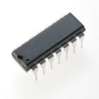
NJM567M-TE1 NJR, NJM567M-TE1 Datasheet - Page 6

NJM567M-TE1
Manufacturer Part Number
NJM567M-TE1
Description
Telephone Ringers _
Manufacturer
NJR
Datasheet
1.NJM567M-TE1.pdf
(10 pages)
Specifications of NJM567M-TE1
Mounting Style
Through Hole
Operating Supply Voltage
36 V
Package / Case
DIP-14
Minimum Operating Temperature
125 C
Lead Free Status / RoHS Status
Lead free / RoHS Compliant
Available stocks
Company
Part Number
Manufacturer
Quantity
Price
Part Number:
NJM567M-TE1
Manufacturer:
JRC
Quantity:
20 000
transistor saturates; its collector voltage being less than 1.0volt (typically 0.6V) at full output current (100mA). The voltage
at pin 2 is the phase detector output which is a linear function of frequency over the range of 0.95 to 1.05 f
of about 20mV per percent of frequency deviation. The average voltage at pin 1 is, during lock, a function of the inband
input amplitude in accordance with the transfer characteristic given. Pin 5 is the controlled oscillator square wave output
of magnitude (+V -2V
exponential triangle of 1 volt peak-to-peak with an average dc level of +V2. Only high impedance loads may be
connected to pin 6 without affecting the CCO duty cycle or temperature stability.
■ OPERATING PRECAUTIONS
capable.
1. Operation in the high level mode (above 200mV) will free the user from bandwidth variations due to changes in the
in-band signal amplitude. The input stage is now limiting, however, so that out-band signals or high noise levels can
cause an apparent bandwidth reduction as the in-band signal is suppressed. Also, the limiting action will create in-band
components from sub-harmonic signals, so the 567 becomes sensitive to signals at f
2. The 567 will lock onto signals near (2n + 1) f
Thus, signals at 5f
before reaching the 567 input.
3. Maximum immunity from noise and outband siganls is afforded in the low input level (below 200mVrms) and reduced
bandwidth operating mode. However, decreased loop damping causes the worse-case lock-up time to increase, as
shown by the Greatest Number of Cycles Before Output vs Bandwidth graph.
4. Due to the high switching speeds (20ns) associated with 567 operation, care should be taken in lead routing. Lead
lengths should be kept to a minimum. The power supply should be adequately bypassed close to the 567 with a 0.01µF
or greater capacitor; grounding paths should be carefully chosen to avoid ground loops and unwanted voltage variations.
Another factor which must be considered is the effect of load energization on the power supply. For example, an
incandescent lamp typically draws 10 times rated current at turn-on. This can cause supply voltage fluctuations which
could, for example, shift the detection band of narrow-band systems sufficiently to cause momentary loss of lock. The
result is a low-frequency oscillation into an out of lock. Such effects can be prevented by supplying heavy load currents
from a separate supply or increasing the supply filter capacitor.
◎ Output Terminal(Fig.2)
- 6 -
The primary output is the uncommitted output transistor collector, pin 8. When an in-band input signal is present, this
A brief review of the following precautions will help the user achieve the high level of performance of which the 567 is
O
and 9f
be
) ≈ (+V -1.4V) having a dc average of +V/2. A 1kΩ load may be driven from pin 5. Pin 6 is an
O
can cause an unwanted output. If such signals are anticipated, they should be attenuated
O
, and will give an output for signals near (4n + 1) f
Figure 2
O
/ 3, f
O
/ 5, etc.
O
where n = 0, 1, 2, etc.
O
Ver.2003-12-09
with a slope


